Steep learning curves in RF mmWave antenna design demand collaboration and technology understanding beyond sub-6 GHz strategies.
5G shifts us from the connected era to the data era. Where wireless strategies were once about connecting everything, 5G delivers information and empowers services that improve our lives. For engineers and designers, this advancement comes at the cost of increased complexity, unique engineering challenges, and critical design considerations.
Mobile carrier build-outs focus on both sub-6 GHz and millimeter wave (mmWave) spectrums. The spectrums are, however, inherently different in terms of engineering, performance, deployment, and purpose. Antenna design, manufacturing processes, RF leakage, and a dearth of engineering expertise contribute to 5G’s deployment challenge.
Sub-6 GHz frequencies easily coexist with LTE technologies. The “sub-6” spectrum is integral to mobile carrier networks. Some equate sub-6 to high performing LTE, with faster data rates and more geographical endurance than mmWave. Unlike mmWave, sub-6 transmits through buildings, walls, and terrain — real-world characteristics that challenge mmWave performance. On this landscape, sub-6 sacrifices speed for signal consistency. Compared to sub-6 signals, mmWaves don’t travel as far. Buildings, trees, people, and even weather can interfere with mmWave signal integrity.
Designing for mmWave-based 5G requires attention not only to the antenna but also to the feeds, traces, and connections that go into that antenna, which must be designed to efficiently handle frequencies above 40 GHz. End-to-end signal integrity is necessary for every high frequency 5G device and critical to defining how well devices perform and utilize ultrahigh-speed 5G signals.
The progression of 4G devices is a good example. New materials, introduced for use in the flexible printed circuit (FPC) signal transfer lines and the antennas themselves, shifted from polyamides to liquid crystal polymers (LCPs) and then again to a modified polyamide. These transitions affect cost and attempt to reduce signal loss. LCP and modified polyamide components save space in the phone design. Their bendable, flexible nature enables better routing. Add to the mix mmWave speeds that are 10-100x faster, and it becomes apparent that antenna designers must design for the whole solution to ensure signal integrity.
mmWave antenna considerations
Where sub-6 relies on non-array antennas (more traditional omnidirectional monopole/dipole style), mmWave requires array antennas, a type most often used in military or scientific applications. Many antenna engineers lack expertise in deep space radar communications. Even with a solid understanding of antenna engineering, engineers need a deeper skillset, one that includes beamforming and beam steering that further increases design complexity, or at the very least ensure its vast difference from more traditional antenna design. (See Figure 1.)
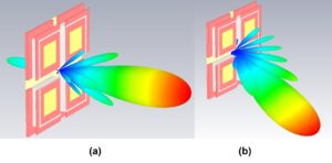
Figure 1. Beam-steering changes the direction of the antenna array’s beam maximum from (a) broadside to some angle away from broadside (b) with the purpose of “finding” a cell site or user. (Click image to enlarge.)
mmWave’s higher frequencies mean its components are more sensitive to frequency and temperature, which can cause antenna detuning. Materials can affect performance of antennas and other components in proximity on a device. Further, meeting 5G performance will require more than one array, so there are multiple systems competing for space in small devices.
Make smarter material choices
At the same time, the number of interconnects and antennas inside these devices has vastly increased, causing pressure for new thinking in how they are engineered. This is especially true as device manufacturers fail to offer relief on the necessary specs. Specs are increasing in terms of performance demands even as device manufacturers reduce costs. Engineers must move away from materials unfriendly to mmWaves.
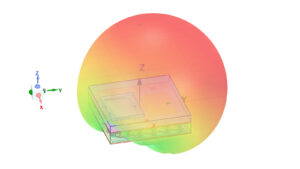
Figure 2. An overlay plot shows the far-field gain of an antenna in package (AiP) designed with high yield manufacturing.
Furthermore, engineers must evaluate manufacturing processes for RF interconnects and antennas. Designs are moving away from traditional PCB integrated or polyimide flexible circuit transmission lines and PC/ABS antennas. Instead, engineers opt for plated plastics, molded and laminated materials made from low-loss LCPs. Moves to stamping, forming, and molding let engineers replace more expensive components with lower-cost components that may be friendlier for processing; however, engineers must be sure to select the correct dielectric materials (Figure 2). High-quality designs will incorporate low loss, low dielectric constant (Dk) substrates, creating direct value in antenna efficiency by minimizing thermal and dielectric loss. For example, in a massive MIMO (multiple-input and multiple-output) deployment featuring 32 transmit and 32 receive signals, the actual power per channel or per signal is very low and therefore transmission loss becomes critical. Here, you must balance any desire to use molded materials with the substance’s inherently higher dielectric constants — a fine line to meet in achieving top performance through use of a lower-cost material. Creating a high precision simulated structure is a crucial step and requires knowledge of all material properties for accurate results.
Simulate surface roughness and antenna-covering sensitivity
In addition to simulating dielectric properties of a substrate, simulation tools, using a microwave simulator, can model surface roughness of conductors early in the design process. From the simulations, you can understand the level of accuracy required. Simulation of various mmWave applications demonstrates the advantage of suitable surface roughness; when shifted to a degraded level, antenna efficiencies drop dramatically. Even variations as small as tenths of a millimeter in size may create significant performance changes. While design models and plating materials must be carefully considered and simulated for performance value, the process also reduces product iterations and accelerates development timelines. For evolving 5G, this is another potential hurdle for engineers accustomed to the inherent forgiveness of sub-6 GHz frequencies.
Antenna coverings used in macro and small-cell base stations also require special consideration because mmWave elements are very sensitive to these materials. Reflections and interference may result when the antenna attempts to radiate mmWave transmissions through the substance. Materials must be kept very thin and with a low Dk, as reflections then tend to be smaller amplitude. Ideally, covering material must be highly fractional in terms of its thickness compared to the wavelength in use. As mmWave designs move higher in frequency, enclosure thickness poses more potential interference on the waves moving through the antenna. In contrast, sub-6 GHz has very little interaction with enclosures; it does affect where its waves resonate, but with much less reflection and loss compared to mmWave.
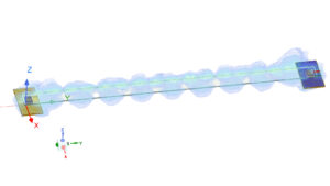
Figure 3. A simulation model demonstrates the electric field leakage from a long RF transmission line flexible circuit and a pair of PCB-mounted connectors.
Multiple radios in a single device
5G engineers must consider the full architecture of a device, as sub-6 GHz and mmWave are implemented along with Wi-Fi, Bluetooth, NFC, and UWB. The addition of the 5G radio in an already crowded device creates new requirement levels for RF leakage in that device. Performance is a concern, as is placement of each individual component (Figure 3). As engineers address mmWave and its unique challenges, the system must not leak energy into the rest of the device, potentially affecting performance of other frequency bands. This requires deeper and more careful consideration of the RF chain, from modem to the mmWave antenna’s front end. From an engineering perspective, this need has translated to a stronger and more fine-grained focus on improvements to RF shielding and digital interconnects as well as transmission line systems. Increasingly demanding design specs speak to this need, driving further emphasis on collaboration among design teams.
Engineering teams must work together, simultaneously evaluating all aspects of a design. Even as signal integrity teams address connector, interconnect, and transmission line performance for power and loss, electromagnetics staff studies the design’s broad impact on RF leakage. This can be a highly iterative process, heavily reliant on constant communication. One design edit may improve signal integrity but demand a trade-off to manage or reduce RF leakage. Precision manufacturing must then maintain tight tolerances. It’s a design process that has the potential to involve every team from mechanical and signal integrity to electromagnetics and molding specialists.
To combat design pitfalls, 5G engineers are rethinking the design process and engineering team structure. Groups that can tap into a diverse industry presence are well-positioned, blending design capabilities in high-speed connectors, antennas for base stations, and consumer device connectivity to complete a more holistic view of 5G. Engineers from the antenna group, as well as the board-to-board or board-to-FPC designers, might have once worked in isolation. Today, these groups must not only be more collaborative amongst one another but with their customers. Historically, consumer device developers have waited until late in the process to determine antenna design and placement. This is no longer an option. Serious consideration of mmWave strategies must happen much earlier, which may even reveal that an existing sub-6 GHz technology provider may not have the depth to seamlessly integrate mmWave advances.
Engineers also need a different mindset from the customer. The evolution of their product design may or may not have been purely straightforward before involving the engineering groups. Sharing this kind of insight can help define the design’s direction, even as the engineering groups can in turn create impact based on their larger industry experiences. Constant interaction and feedback require a willingness to share lessons learned and create communication channels that remain open throughout the design process. This does represent a higher bar for customers, who may find themselves challenged to meet it by more experienced, insightful and therefore more demanding engineering teams. Handing over a spec is not sufficient, and the design and engineering groups in the mix will make clear their expectation for customers to see and participate in the full development process.
Ideally, collaboration across departments, business units, and teams begins early in the design process. Such collaboration can build long-term, trusted relationships through shared simulation files, routine meetings among front-end and back-end teams, and constant formal and informal feedback.
5G is different – for mobile carriers, designers and engineers, and end user customers. Antenna designers, microwave circuit designers, even those designing devices and considering adding mmWave functionality, must embrace significant cost and steep learning curves for understanding and implementing these technologies. But even as mmWave rollout timelines are longer, the industry is benefitting from time spent developing and releasing more cost-competitive hardware options, as well as refining solutions that solve deployment challenges such as signal integrity. This is a long-term advantage, coupled with greater clarity on how to execute smart, collaborative 5G designs, and is poised to drive mmWave further and expand its capabilities.
 Tim Gagnon is a Principal RF Design Engineer driving development in antenna, micro-connector and RF IC solutions at Molex. He has more than 20 years’ experience in wireless solutions, focusing on customizing and implementing general market or unique solutions for customers in consumer, medical and automotive industries. Tim has his bachelor’s degree from Georgia Tech and his master’s from UMass Amherst. Connect with Tim at Tim.Gagnon@molex.com or LinkedIn.


Tell Us What You Think!