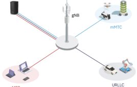
To enable the large increase in wireless data transfer needed for the new 5G wireless standard, spectrum in the millimeter wave (mmWave) range will be needed. There is simply not enough available spectrum in the sub-6 GHz range. The mmWave range is largely unregulated with wide chunks of available bandwidth making it ideal for data transfer applications.
As in lower frequency applications in the RF/microwave bands, control of electromagnetic interference (EMI) is critical in the mmWave bands. Traditional shielding techniques are less effective due to smaller wavelengths. A gap in a shield that is negligible at 3 GHz becomes large in terms of a wavelength at 30 GHz. While higher tolerance manufacturing techniques can mitigate this somewhat, the use of absorbers for EMI control in the mmWave range is critical.
What can absorbers do at mmWave?
Antenna Isolation
Some 5G systems will use massive MIMO techniques to enable high gain antenna beams and to increase spatial multiplexing. These antennas will consist of arrays of anywhere from 16 to 128 antenna elements that will act as a phased array to steer antenna beams. Since each antenna element will act as both a transmitter and receiver, it is critical to isolate the elements from each other to prevent the (relatively high power) transmitted signal from one element to leak into the receive portion of an adjacent element. This is difficult to do effectively with shielding alone. An absorber material with the correct properties would be ideal to reduce this cross talk and also to eliminate reflections from other parts of the device which could interfere with the desired signal.
Board Level Shield Cavity Resonance
Board level shields will still be a key part of an EMI mitigation plan at mmWave. However, care must be taken reduce the impact of cavity resonance. Cavity resonance occurs when a conductive enclosure is larger than half a wavelength. Energy can then oscillate (or resonate) inside the cavity, potentially affecting circuit operation inside the cavity and increasing shielding leakage at the cavity resonance frequencies. The existence of a cavity resonance depends on both the frequency and the size of the cavity. At 2 GHz, the shield would need to have a dimension of 7.5 cm (half a wavelength).
This is rather large for a shield, hence cavity resonance is rarely an issue at these low frequencies. At 30 GHz, however, a shield as small as 5 mm could exhibit a resonance.
To maintain the shielding effectiveness of a board level shield that exhibits a cavity resonance, a thin layer of absorber material could be applied inside the shield. The electromagnetic parameters (permittivity, permeability) of absorber material are related to energy storage of the electric and magnetic fields. When added inside a cavity, solving the field equations shows that the energy tends to reside in the high permittivity/permeability material. The energy will resonate inside the absorber where it will be absorbed.
Millimeter Wave Reflection Reduction
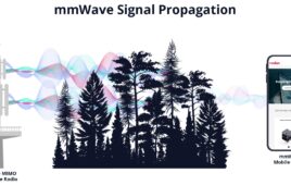
In free space, once the mmWave signal has radiated, objects near the antenna can reflect signal, which will interfere with the desired transmitted signal. Absorbers can be used to reduce or eliminate these reflections.
Absorbers
A range of absorber materials is effective in the mmWave spectrum. Absorbers are available in various forms including polyurethane foams, silicone or urethane elastomers, and in a range of thermoset forms intended for injection molding.
Absorbers consist of two general parts, the container material and the filler material. The key to electromagnetic absorption of a material lies almost entirely in the filler material. The container material serves to suspend and hold the filler in place in to absorb the energy. Absorptive fillers come in two categories, dielectric and magnetic. A dielectric filler absorbs primarily the electric field energy in an electromagnetic wave, while a magnetic filler absorbs primarily the magnetic field. The electric field and magnetic field are coupled so that a reduction in one will result in a reduction of the other. The choice of which filler type to use comes down to what type of energy dominates at the absorber’s location.
For many applications a magnetically loaded absorber may be desirable. Unfortunately, magnetically active filler materials tend to lose their effectiveness above 40 GHz. As a result, dielectric fillers are recommended for that frequency range.
The container material is chosen based on its physical properties or the desired size/shape of the final product. A polyurethane foam may be chosen based on cost or low weight. An elastomer may be chosen for material toughness or other environmental properties are desired. A thermoset material may be chosen for a complex shaped part which is best made using injection molding techniques.
In many circuit designs, the best result is seen when components can be spaced a prescribed distance from each other. Ideally the interposer material would be air but often inclusion of posts to keep the components separate is not feasible. In these instances, a thin sheet of material can be employed. This sheet would provide mechanical support and have a minimal effect on electromagnetic performance. Ideally the dielectric constant (Dk) would be equal to one. Many foam materials can approach a Dk of one but it is often difficult to manufacture foam at the thicknesses needed in designs. Also, foam can often not handle the high temperatures seen in some electronic designs.
In addition, if the spacer material is between two conductive planes, the inclusion of a dielectric will increase the capacitance of those planes, often resulting in unacceptable coupling or other effects. The capacitance is directly proportional to the dielectric constant.
As frequencies increase, there will be a greater need for absorber material to achieve EMI/EMC goals. Accurate parameter measurement is key to characterizing material properties for use in electromagnetic modeling software.
Parameter Measurement
Full characterization of absorber material depends on accurate measurement of the permittivity and permeability as a function of frequency. Permittivity (?) is a measure of the material’s response to the electric field. Permeability (μ) is a measure of the material’s response to a magnetic field. Knowledge of ? and μ enables accurate prediction of absorber performance in electromagnetic modeling.
Permittivity and permeability are complex numbers. The real portion of each relates to the amount of electric/magnetic energy storage and wavelength compression in the material. The imaginary portion of each relates to the amount of electric/magnetic loss in the material.
In order to measure the complex permittivity and permeability of absorber material, the reflection coefficient and transmission coefficient of a sample of known thickness must be measured. These coefficients are themselves complex and represent the magnitude and the phase of reflection and transmission measurements.
To allow precise measurements of magnitude and phase, parameters are usually measured in ‘closed’ systems such as coaxial lines or waveguides. This enables controlled incidence angles of the energy upon the material and in the case of waveguides, known electromagnetic properties of the energy hitting the material.
A primary difficulty in measuring parameters is sample preparation. In the RF/microwave frequency band, parameter testing is straightforward using waveguides and coaxial lines. A 1 in. diameter line can be used up to 6 GHz. A 7 mm diameter coaxial line can be used up to 18 GHz. While waveguides can be rather large at frequencies below 6 GHz or so, rectangular samples are relatively easy to fabricate compared to coaxial samples.
Full parameter characterization requires accurate measurement of reflection and transmission of a material
In the mmWave band, machining samples for coax or waveguide becomes progressively more difficult as the frequency increases. A 7 mm line will begin to see multimode affects at 18 GHz. A 3.5 cm line will see multimode affects at about 36 GHz. Coaxial samples are too small to machine accurately at these frequencies so waveguides must be used, but waveguides also have size limitations. A waveguide to cover the 18-26.5 GHz band is 10.7mm x 4.3mm. To cover 26.540 GHz reduces the needed sample size to 7.1mm x 3.6mm. Here the issue becomes not only the small sample size, but precision calibration standards are more difficult to fabricate.
Beyond 40 GHz, sample size and difficulty in calibration standards precludes coax/waveguide parameter measurements. Free space techniques must be used.
In free space it is difficult to guarantee that the signal impinging on the sample is a plane wave. At lab distances, the signal from most antennas is still somewhat spherical which will greatly add to measurement error. Gaussian beam horn antennas are used. Precision machined reflectors are used to generate a plane wave at the sample location. The quasioptical bench enables precision full parameter measurement and characterization up to 67 GHz.
Conclusion
An ability to measure and characterize material parameters of absorber in the mmWave band up to 90 GHz is mandatory. Accurate material parameters measurements are essential to ensuring excellent absorber performance in demanding high frequency applications.