We live in an interconnected world, where mobile communication plays a huge role. This increasing demand for high-speed, low-latency networks are defining fifth-generation (5G) mobile connectivity, which are driven by changing user demands, the Internet of Things (IoT), and Industrial Internet of Things (IIoT). Both introduce machine-to-machine communication, require reliable networks, and low-latency response times for critical applications. 5G networks challenge operators and equipment OEMs as different frequency bands across geographic locations and regulatory environments, presenting the need to support multiple air interfaces requiring adaptable solutions.
Therefore, 5G networks are defined by their ability to increase reliability connections with significantly reduced latency at increased data rates, while providing greater capacity and support for increased connection numbers. 5G solutions must provide the cornerstones of increased spectral efficiency and support for ultra-densification. Increased spectral efficiency enables more information to be transferred within a fixed bandwidth for addressing increased data rate and capacity demand. While ultra-densification provides significant increases in base stations and back-haul connections, it also offers implementation capabilities that drive the change in solution.
Current 4G network infrastructure presents several issues limiting its ability to scale and support next-generation networks. These typically consist of antenna arrays and connected radio heads mounted on cell towers, which may provide an integrated radio head and antenna, or distributed approach. To provide better system performance and reduce losses, an integrated approach is used. Even this integrated approach doesn’t provide capacity to implement 5G networks, being unable to support the number of connected devices at the data rates required.
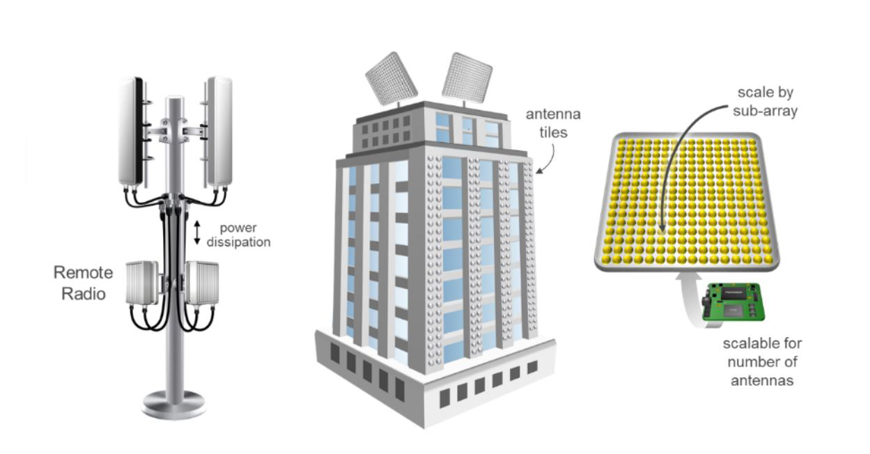
Figure 1: Evolution from 4G Tower to MIMO.
Massive Multiple Input Multiple Output (Massive MIMO) architectures are being considered to provide 5G network infrastructure, consisting of multiple antenna systems (potentially up to 1024 antenna). Therefore, massive MIMO can implement fine grain beamforming and enable spatial multiplexing, meaning each of the beams can support the full bandwidth. Massive MIMO solutions also enable messages to be broken up and transmitted simultaneously over different paths.
This change allows for ultra-densification as antenna tiles are deployable on buildings, structures, and other surrounding infrastructure moving away from the cell tower. This change also brings constraints on the connected radio unit, hindering both energy efficiency, form factor, and scalability from small- to large-scale antenna deployments.
Embedded System Level Challenges
To support small antenna deployments, the radio architecture core must be tightly integrated. The traditional approach would be combining multi-giga sample ADCs and DACs with a System-on-Chip (SoC). This approach provides the ability to perform the embedded system design; e.g., virtualization, CloudRAN, etc., within the SoC processor cores, while programmable logic implements ADC/DAC interfaces and signal processing pipeline.
This approach requires significant board space to implement the SoC with supporting peripherals, and analog front-end containing the DAC and ADC. To ensure RF performance isn’t compromised, separation between devices must be maintained along with following stringent time-consuming layout rules. The more channels required, the more complex addressing routing signals and power integrity becomes. To address the increased required operating bandwidths, many data converters implement interfaces using JESD204B.
Typical high-performance ADCs may require 2.25 W, while DACs would be in the order of 1.75 W. This both increases required board space required, and power dissipation of the overall solution. Additional steps required in the design increase time taken for development—increasing the non-recurring engineering, and development costs, along with manufacturing and bill of material expenses.
To solve challenges presented by the network operator licensing and geographical restrictions, using direct RF sampling reduces required analog front-end components. Direct sampling is enabled by using ADC and DAC devices with a high sampling frequency and wide analog input bandwidth. This removes the need for analog front end, down converting the signal into the ADC sampling window. Their design requires specialized skills and careful consideration of the component selection, placement, and routing.
The designer must also consider component drift with aging and temperature. Direct sampling removes the need for many components, allowing processing to be performed within the digital domain. It does come with a trade-off of higher sampling discrete ADC and DAC required for directly sampling RF signals have higher power dissipations.
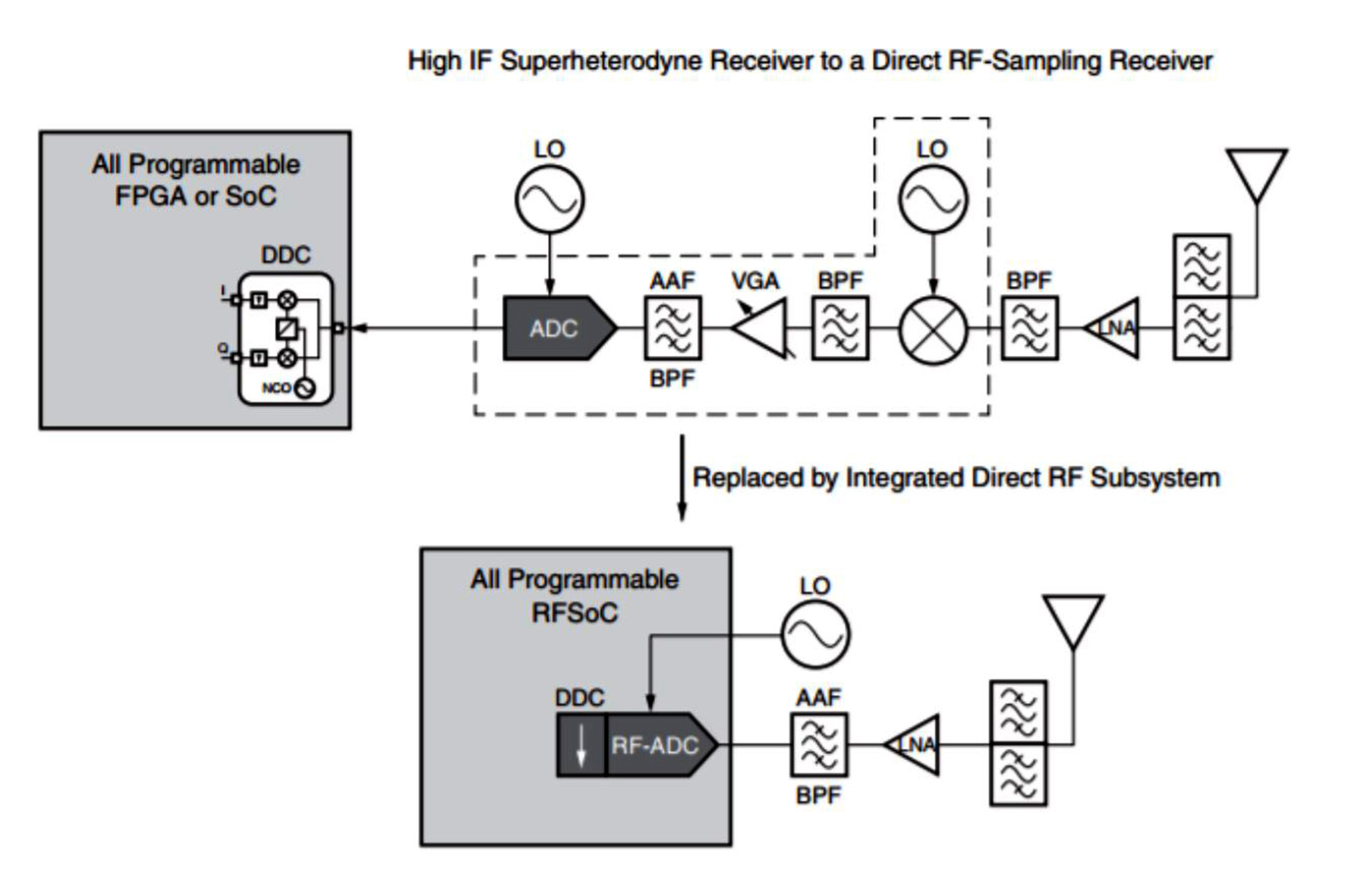
Figure 2: Direct vs. IF Conversion.
RFSoC Concept
The RFSoC concept integrates the multi-giga sample ADCs and DACs within the same silicon as the SoC, containing the processing system and programmable logic. This offers a tighter integrated solution (while providing a direct sampling RF solution for 5G applications). Integration of ADC and DAC, isn’t on its own, sufficient to address the challenges. The RFSoC must contain mixers, numerically controlled oscillators, phase, and support real or in-phase and Quadrature formatting.
The tightly integrated RFSoC concept enables the device to offer a reduced board area when compared to similar discrete solutions. A typical DAC or ADC may require up to 15 mm x 15 mm of board space. An application, which requires eight converters of either type, would therefore require 1800 mm2. A similar solution could typically fit in 30 mm x 30 mm packaging, requiring only 900 mm2 of board space.
Providing this tightly integrated solution reduces the required board area, and overall power dissipation. As energy scales with sampling frequency, reductions provided by tightly integrated solutions become apparent (Figure 3).
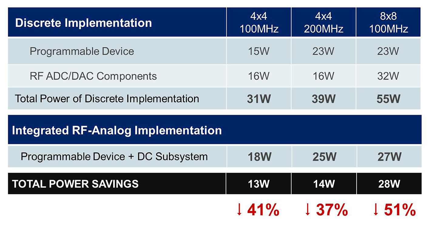
Figure 3: Power reduction provided by the RFSoC concept.
Such a device offers significant reductions in the complexity of sample clock distribution. The simpler network reduces the power and cost associated with distributing GHz clocks on the PCB, offering a more efficient solution.
Analog Performance
Traditionally, high-performance analog circuits like ADC and DAC haven’t used advanced CMOS technology for implementation. With digital assistance, it’s possible to implement high-performance converters using 16 nm CMOS FinFET technology. Two test chips were developed to examine the potential RF/Analog performance. The first implemented an ADC and digital circuitry, while the second deployed a DAC convertor and its digital circuitry. The ADC test chip implemented a three-stage asynchronous pipelined SAR with open-loop integrator-based amplifiers (Figure 4).

Figure 4: (a) Overall architecture (b) ADC topology.
The selected architecture allows maximization of the sampling frequency, resolution, and linearity. To ensure reduced power, noise, and cost, the architecture is supported by several dynamic circuits and multiple digital calibration loops. The ADC design is configurable to support either dual-channel conversion using inputs In0 and In2 (Figure 4), or a single-channel conversion. This approach enables the ADC to support either direct RF or I/Q architectures. Using the 4 GSPS sampling rate provides more flexibility within frequency planning, as it supports a wider bandwidth. Each 2 GSPS ADC slice contains four 500 MSPS ADCs, which operate in an interleaved manner.
The results for this ADC test chip at 4 GSPS in direct RF mode are INL +/-1.5 LSB and DNL +/-0.3 LSB. While applying an input of -1dBFS signal at 1.9 GHz, the convertor provides a SFDR of 67.0 dB and SNDR of 57.3 dB, while total power at 4 GSPS is 513 mW.
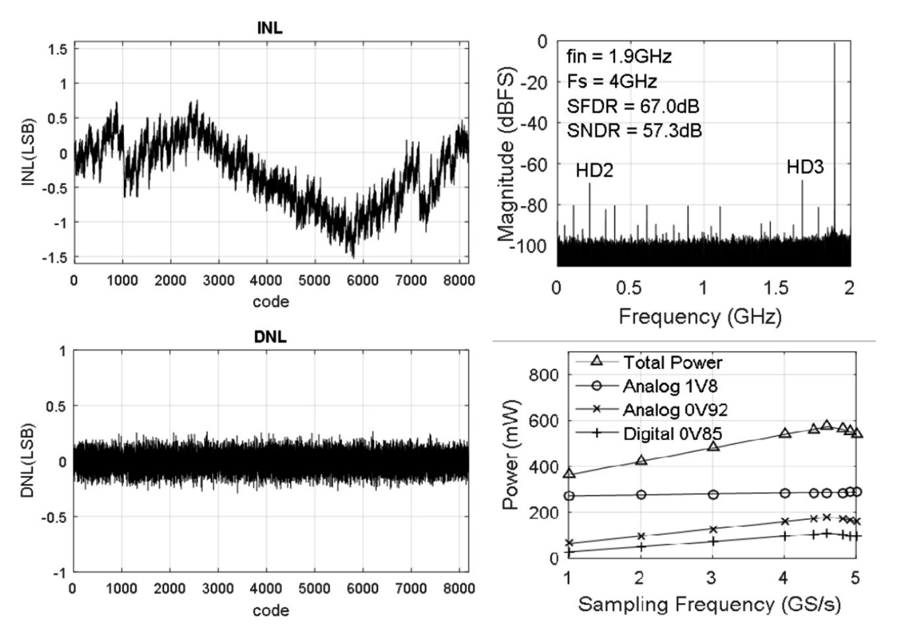
Figure 5: INL, DNL, FFT, and Power.
How Does RFSoC Address These Challenges?
Addressing 5G-related challenges requires the capability to implement systems that support increased spectral efficiency and ultra-densification. This requires the ability of the 5G radio to offer a low-power, compact, high-performance system. This solution also must also scale with the number of antenna being supported.
The concept addresses these challenges, providing a significant reduction in the solution footprint to implement a small radio when compared to a discrete implementation of circa 50 percent. As the number of antenna supported by the system and signal BW increases, so do the required JESD links between SoC and external convertors. This space saving becomes more significant thanks to the RFSoC integration. This reduction enables the current proof of concept implementations to become more commercially viable.


