In virtually every RF and microwave system, a frequency synthesizer is required. The frequency synthesizer creates the local oscillator signal that drives mixer, modulators, demodulators, and many other RF and microwave components. One way of creating a synthesizer, often considered the “heartbeat” of the system, is using a Phase Locked Loop (PLL) frequency synthesizer.
Traditionally, a simple PLL is divided down the Voltage Controlled Oscillator (VCO) output frequency, compared to a reference signal, and then the VCO is tweaked to control voltage to tweak its output frequency. For many years, the PLL and VCO have been two separate chips—a discrete solution. The VCO creates the actual output signals; the PLL monitors the output signals and tunes the VCO to lock it relative to a known reference signal.
There are a number of strengths to the discrete solution:
- Each discrete chip can be designed to give its best possible performance.
- The physical distance between the PLL and the VCO reduces cross-coupling effects and minimizes unwanted spurious signals on the output.
- If one chip in the loop is damaged, less components need to be replaced.
Discrete solutions have dominated the synthesizer industry for a long time, but there were also downsides. One major issue is that the discrete solution requires a lot of board space to hold the two chips and all their supporting components. This resulted in larger-end products and higher cost.
Another major issue with the discrete solution is that traditional VCOs have a narrow output frequency range. A typical VCO bandwidth is 50 to 500 MHz; it’s possible to go up around 2 GHz, but this requires an op-amp based active filter. This is a major challenge for anyone who wants to implement a system with a wider frequency range. To create a wider frequency range synthesizer, multiple PLLs, VCOs, supporting components, filtering, switches, and power supplies are needed. This exponentially increases the board space and cost of a design. Not only do discrete solutions impact the board design, but there is also a huge amount of overhead work in qualifying, creating software for, and controlling inventory for each device.
About 10 years ago, there was a breakthrough in the PLL-based synthesizer industry. The first integrated PLLs and VCOs (PLL/VCO) started to appear on the market. This major development meant boards could be smaller, cost lower, and reduced overhead dramatically. The integrated solution also meant the VCO architecture could change to create a wideband synthesizer from one component. Let’s explore the VCO architecture and how the shift to integrated VCOs opens doors in synthesizer performance.
Traditional VCOs are simple devices. A voltage is applied to a tuning pin on the VCO, and a certain frequency is output; the voltage is increased, and the output frequency increases; the voltage is decreased, and the output frequency is decreased. Figure 1 shows the tuning voltage vs. output frequency of a GaAs MMIC VCO: the 13 V tuning range requires an active filter or a PLL with a high voltage charge pump.
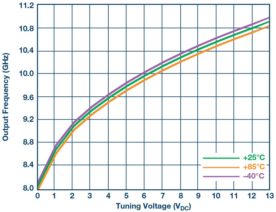
Figure 1. Traditional VCO – tuning voltage vs. output frequency.
The integrated PLL/VCO solution uses a different type of VCO architecture that builds on the traditional architecture. The integrated PLL/VCO effectively combines several traditional VCOs side-by-side to create a VCO with a remarkably wide bandwidth. Each individual VCO, created by switching capacitors in and out, are called bands. The fact that the PLL and VCO are integrated onto one chip makes the multiband architecture possible. Every time the user wants to lock to a new frequency, the device initiates a VCO calibration process where the chip quickly sorts through the VCO bands and chooses the optimum one for the required output frequency. Once the VCO band has been selected, the PLL then locks the loop and keeps the output at the desired frequency.
The first generation of these PLL/VCO chips had over 4 GHz of bandwidth. Compare that to the discrete 100 to 300 MHz bandwidth; a tiny chip made this frequency range possible, relative to the previously required banks of PLLs, VCOs, filters, and switches. Figure 2 shows the tuning voltage vs. output frequency of a multi-band PLL/VCO. In this example, the fundamental VCO output range was specified as 2200 to 4400 MHz. This was complemented with a bank of dividers after the VCO output but internal to the chip, which could divide the signal to as low as 35 MHz; hence the >4 GHz bandwidth—all from one 5 mm × 5 mm package.
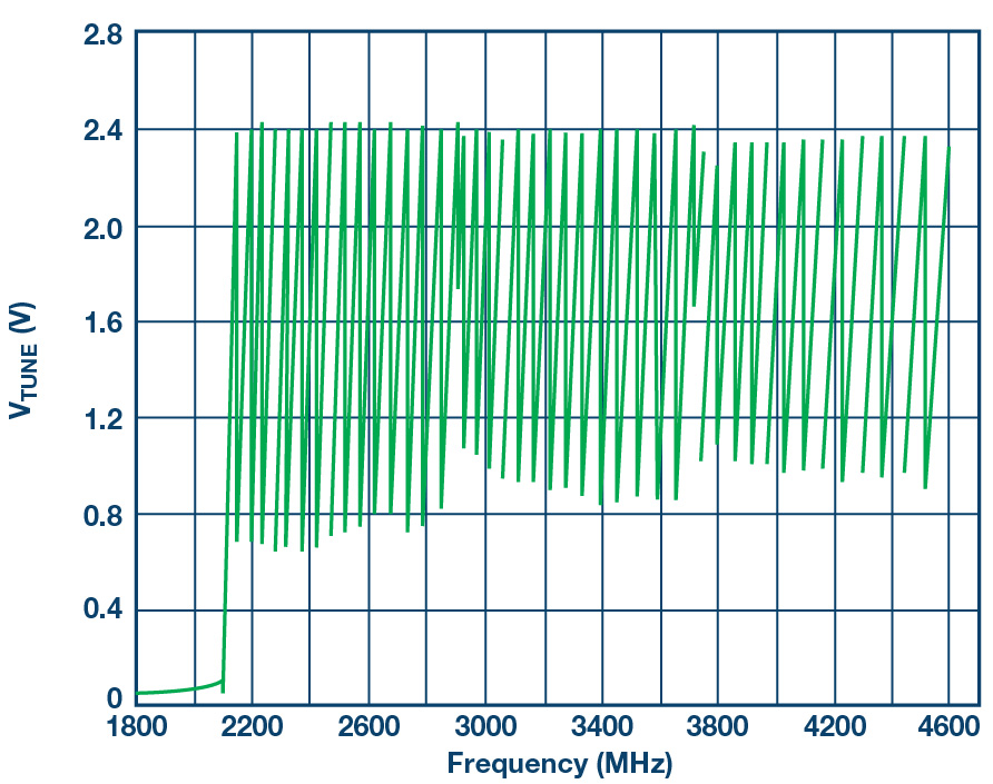
Figure 2. Multi-band VCO – tuning voltage vs. output frequency.
While this breakthrough technology was a huge step forward in frequency range, board space, cost, and overhead, there were still drawbacks that stopped the integrated solution from completely taking over the discrete solution. In many applications, the most important performance specification (after frequency range) is phase noise.
Why is phase noise so important? Imagine a system were a signal is transmitted over clear air. Say the signal-to-noise ratio of the transmitted signal is 50 dB at the transmitting antenna; that means, the signal the receiver to supposed to receive is 50 dB more powerful than the noise on either side of the transmitted signal, i.e. at nearby higher and lower frequencies. Let’s say this signal can travel 10 miles before the signal power is decayed into the noise, and the transmission is lost. Now, suppose the phase noise of the synthesizer is improved by 3 dB. This means the signal-to-noise ratio of the transmitted signal is 53 dB. As a result, the transmitted signal power is twice that of the previous 10 mile range signal and can therefore travel farther before it decays into the noise. More distance means less repeaters/transmitters are needed, and costs can be reduced.
Beyond this communications example, there is an additional drive for phase noise performance from the electronic test and measurement community. Whatever phase noise performance is used by the communications industry, the electronic test and measurement instruments need better phase noise performance so they can measure the communications protocols.
While many solutions were able to move from discrete to integrated (saving millions of dollars in the process), the phase noise performance of the first generation PLL/VCO simply wasn’t good enough to replace many of the low-phase-noise requirement applications. As well as the phase noise performance, the frequency range was still pretty low compared to many of the applications that require a discrete PLL and VCO.
The frequency range issue can be mitigated by frequency doublers and other multipliers, but these are power hungry and add additional cost and board space to the solution.
Fortunately, while these integrated solutions were being rolled out, development was already underway to move to new IC processes, which allowed for the much sought after phase noise and frequency range improvements.
So, at this point, the stage is set for the second generation of integrated PLL/VCO. The requirements are:
- Output frequencies greater than 4.4 GHz.
- Phase noise performance comparable with discrete solutions.
- Integrated PLL and VCO in a single small package.
- Lower cost than discrete solutions.
Late 2014 saw the start of this second generation of integrated PLL/VCO. Products started to appear on the market with greater than 10 GHz output frequency range, phase noise comparable to a discrete VCO, 5 mm × 5 mm packages, and lower prices than similar discrete PLL and VCO solutions (which would have a much narrower frequency range).
Now, a user could have all the phase noise performance benefits of a discrete solution, plus all the other benefits of an integrated solution. As an added benefit, PLL technology has also developed over the years, so this second generation of PLL/VCO devices had an assortment of PLL performance enhancements too.
For the first generation of PLL/VCO, the PLL blocks had maximum Phase Frequency Detector (PFD) frequencies around 32 MHz and fractional-N divider resolutions of around 12 bits. This combination meant typical channel resolution was in the tens of kilohertz. The second generation of PLL/VCO has maximum PFD frequencies greater than 100 MHz and fractional-N divider resolutions of 25 bits—or even up to 49 bits. This saw two main benefits: the higher PFD frequency allowed for lower PLL phase noise (every doubling of PFD frequency means the N divider can be halved, so the N divider noise contribution drops by 3 dB); and the 25 bit or more resolution allows exact frequency generation and sub-Hz channel spacing.
Spurious Performance
There is an important aspect of the integrated PLL/VCO that needs to be discussed. One of the benefits of the discrete solution listed above is that the physical isolation between the two chips reduces cross coupling between the PLL and VCO and therefore reduces the power of unwanted spurious signals. When the PLL and VCO are integrated, it is inevitable that the spurious performance will degrade. Some parts in the market managed to keep this degradation very low and have surprisingly good spurious performance for a PLL/VCO. Other PLL/VCO parts need extra applications work to improve the spurious levels for some high-performance products.
Varying the PFD Frequency to Eliminate Integer Boundary Spurs
One technique is to vary the PFD frequency of the PLL using a frequency planning algorithm. This can move spurious signals, caused by the PFD block, to a region where they don’t have a strong impact and are virtually eliminated.
Isolate the PLL and VCO
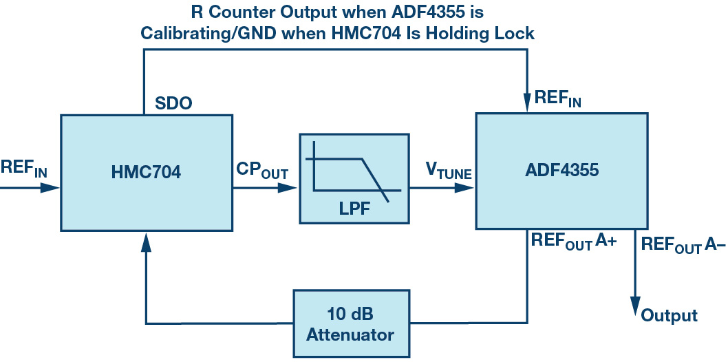
As mentioned above, the close proximity of the PLL and VCO circuits can result in unwanted coupling. To mitigate this, it is possible to use a two-chip solution to physically separate the PLL and VCO circuits. This gives the discrete advantages of low spurious signals and the integrated advantages of a wide output frequency range. To implement this two-chip architecture, the integrated PLL/VCO RF output must be fed to an external PLL’s RF input. The external PLL’s charge pump output goes to a loop filter whose output goes back into the integrated PLL/VCO at the VCO tuning port. Initially, the PLL/VCO locks the loop, but then, the PLL on the integrated part is disabled and the external PLL maintains lock in the loop. Physically isolating the PLL and VCO in this manner is beneficial because it reduces unwanted spurious coupling and, if the external PLL has better performance, that improvement is seen at the output.
Conclusion
There are more and more integrated PLL/VCO devices appearing on the market every year and each generation is bringing higher frequency operation, wider bandwidth, lower phase noise, lower spurious, and all round better performance. Increasingly, applications that previously required a discrete solution can now be implemented with an integrated PLL/VCO solution – this reduces cost, reduces board space, and, most importantly, makes the RF designer’s job easier!

