
Selecting a printed-circuit-board (PCB) material for a high-frequency wireless power amplifier (PA) involves a number of tradeoffs. Beyond the overall tradeoff of cost versus performance, the different electrical properties of PCBs can have different impacts on how well a PA performs under different conditions. Understanding how these different PCB properties are described in different material parameters can help ease and simplify the task of specifying a PCB material best suited for wireless PA circuits.
Most engineers familiar with PCB materials understand how laminate materials can be selected according to basic parameters, such as dielectric constant or relative permittivity (εr or Dk), and dissipation factor or loss tangent (Df). But many other material parameters can impact both Dk and Df as functions of changing temperature and, consequently, can affect the ultimate performance possible from a high-frequency PA fabricated on a particular PCB material.
For example, temperature coefficient of dielectric constant (TCDk) describes how a material’s Dk changes with temperature; TCDk is analogous to Df in that it can provide tremendous insight into a PA’s expected performance over a given temperature range. The coefficient of thermal expansion (CTE) is another circuit material parameter that is key to providing insight into an amplifier’s performance with temperature. CTE is related to the reliability of a circuit-assembly process (and the different temperatures used in manufacturing a PCB) and the long-term reliability of a PA or other circuit, especially those that must operate over wide temperature ranges. Thermal conductivity is yet another important PCB parameter for PA designers, since it is critical to the thermal management of a PCB and can provide insight into how much heat and power a PA will be capable of handling.
Understanding a PCB’s TCDk can be especially important for PAs, where the power delivered by the amplifier is never 100 percent efficient and will raise the temperature of the circuit. These thermal effects are added to the environmental operating temperatures, and a circuit material’s Dk will change according to its TCDk parameter. In particular, amplifiers that have been developed in laboratory environments under controlled conditions and then faced with in-field operating conditions may experience considerable different thermal conditions in the field, with greater impact on Dk. For a PA, where consistent Dk is vital to maintaining the tightly controlled impedance of the matching circuits that help achieve maximum gain and output power, excessive changes in Dk will result in larger-than-expected changes in impedance in these matching circuits, resulting in gain and output-power variations over temperature for a PA.
As a general rule, the TCDk of a PCB material should be better (lower) than 50 ppm°C, with this as an absolute value. Circuit materials based on polytetrafluroroethylene (PTFE) exhibit poor TCDk values, typically around 150 ppm/°C, which indicates much greater variations in Dk with temperature. As a result, most PTFE-based laminates used for high-frequency applications feature glass reinforcement or are filled with materials that can help maintain the stability of the Dk with temperature. Often, ceramic materials are used as filters; they can alter several properties of the PTFE laminate and greatly improve the TCDk of the circuit material.
Thermoset laminates used for high-frequency circuit applications typically exhibit good TCDk values, again, due to the benefits of filler materials. Figure 1 shows the performance of a filter circuit on different PCB materials and how the filter center frequency for each material changes with changes in temperature. The materials used in this example are commonly used in RF/microwave PCB applications. As a general rule of thumb, materials with higher Dk values typically exhibit high TCDk values, although there are exceptions.
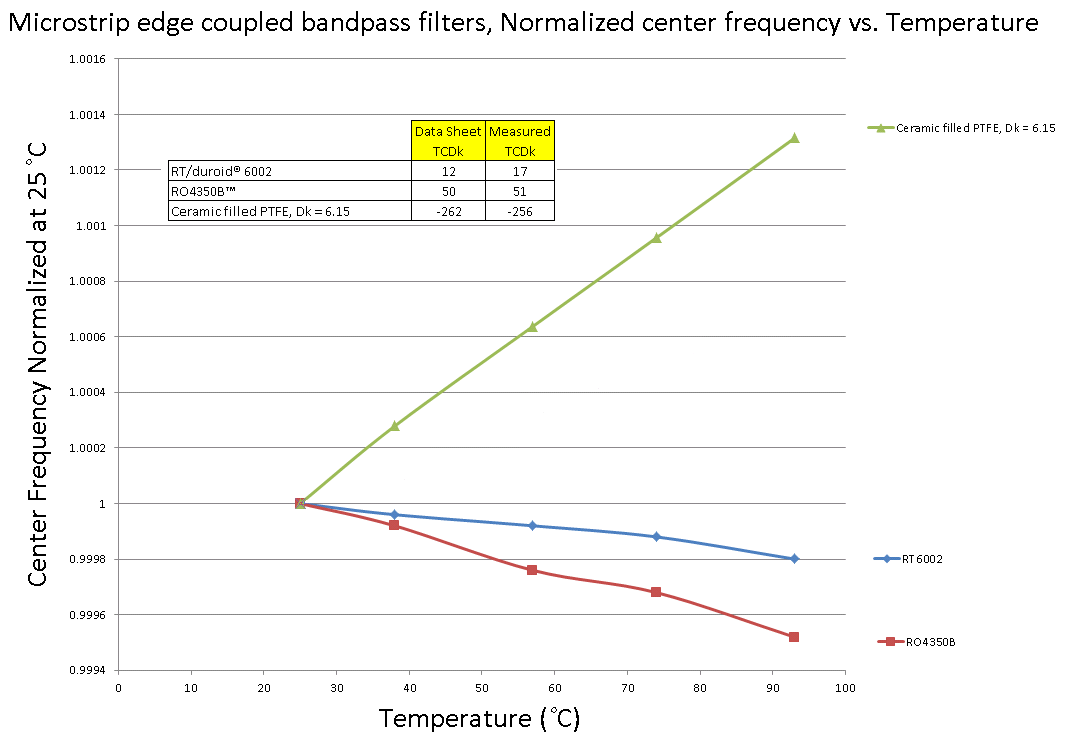
Figure 1: TCDk chart showing three commonly used laminates in the high frequency PCB industry.
For applications where circuit loss is critical, such as to maximize PA gain and output power, a PCB material’s TCDf property is an important consideration. This parameter describes how a material’s loss will change as a function of temperature, typically rising as temperature rises. As with TCDk, the TCDf parameter should be checked for a material under consideration for the requirements of a PA design and for the expected operating environment. Again, in addition to the environmental temperatures, higher-power PAs will add thermal energy of their own, suggesting the selection of a material with TCDk and TCDf values well suited to a wide temperature range.
As noted, thermal conductivity is an important material parameter for high-frequency PA circuits. Most laminates used for high-frequency PCB applications exhibit low thermal conductivity, typically in the range of 0.2 to 0.3 W/m-K. Some laminates are specially formulated for high thermal conductivity, and when combined with good thermal management practices such as the use of heat sinks, can help maintain lower circuit temperatures even for higher-power PAs.
A simple study was performed to show the benefits of circuit materials with higher thermal conductivity values. The experiment involved all two-copper-layer circuits with a termination resistor mounted in the middle. DC power was applied to heat the resistor, and the circuit was mounted on a water-cooled heat sink. Once each circuit reached thermal equilibrium, thermal imaging pictures were taken and heat flow calculations performed. Figure 2 shows the results for circuits with two different thermal conductivity values, 0.25 and 0.64 W/m-K, a common PTFE woven-glass laminate, and a ceramic-filled thermoset laminate, respectively.
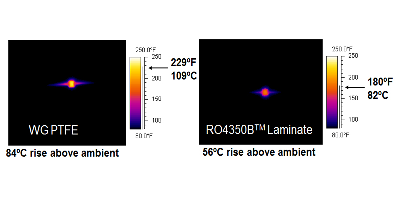
Figure 2: These thermal images represent resistors on circuits being heated by 4 W of DC power. The circuit on the left has a thermal conductivity of 0.25 W/m∙K, and the circuit on the right has a thermal conductivity of 0.64 W/m∙K.
Another experiment was run using a thermoset laminate at a higher power level to compare circuits with and without via farms. A via farm is an array of plated-through-hole (PTH) vias in a PCB that act like thermal conductors beneath a device and efficiently transfer heat from a heat-producing device, such as a power transistor or resistor, to a heat sink below. In Figure 3, circuit material was used with and without via farms at a DC power level of 5 W. The effective power transfer of the via farm is quite apparent.
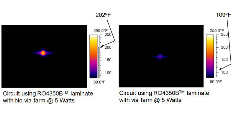
Figure 3: Using the same material, but one circuit design with via farms (right) and the other circuit without (left).
Via farms cannot be used on circuit traces carrying RF power. Instead, via fences may be used to help dissipate heat. A via fence is basically a circuit using grounded coplanar waveguide (GCPW) transmission lines; the vias in the neighboring coplanar ground planes can effectively channel the heat from the signal conductor transmission lines to a heat sink below.
Another important circuit material property related to thermal performance is CTE, which is mostly related to assembly and long-term reliability issues. The value of CTE is much different for different materials and can be a concern for certain applications, including PAs. Pure PTFE materials exhibit high CTE values that are not desirable for applications requiring high reliability. Pure PTFE has a CTE of about 250 ppm/°C, while ceramic-filled PTFE (as mentioned in Figure 1) has a CTE of about 24 ppm/°C. A general rule of thumb for acceptable CTE values would be a CTE of 70 ppm/°C or less. An ideal CTE value would be 17 ppm/°C, or the same value as copper, so that any dimensional changes related to temperature would be the same for the dielectric material and the copper circuit traces on the material. Basically, less stress will build up during thermal cycling in a circuit if the CTE values are the same on the different layers of the circuit.
A key parameter of thermoset PCB materials to consider when fabricating high-frequency PAs is the glass transition temperature, TG. The TG is essentially the temperature at which a material will convert from a more brittle characteristic to having a softer, more elastic property. It is not a maximum operating temperature but rather an upper limit on temperature that a material can endure for only a short time. A material’s TG is linked to its CTE. For example, PCB data sheets may provide a CTE value but not indicate whether that value was determined for the material below or above the TG. A CTE value above the TG or following the TG transition of the material is known as the alpha 2 CTE value, while a CTE value below the TG or before the TG transition of the material is known as the alpha 1 CTE value. An alpha 2 CTE is usually much higher than an alpha 1 CTE for the same circuit material, and it is in the range of temperatures where soldering occurs so it is typically more meaningful. Figure 4 shows a typical TG curve. As can be seen, there are two different CTE trends; one before the TG (alpha 1) and one after the TG (alpha 2).
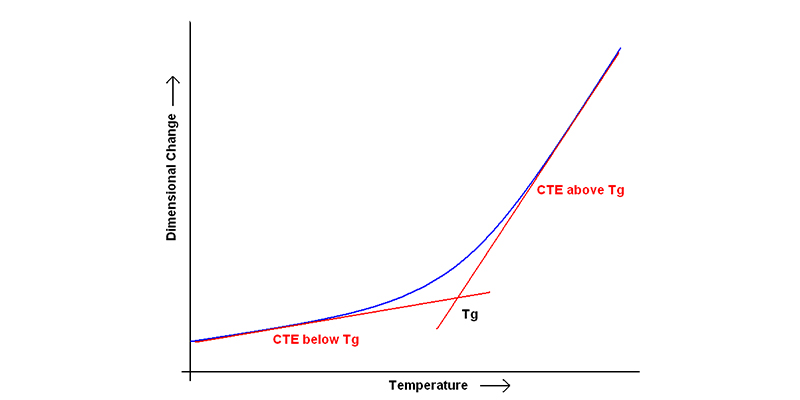
Figure 4: Typical TG curve showing the CTE differences before and after the TG.
Designers concerned with PCB material CTE must be clear on which CTE value is being reported. The alpha 1 values are usually in the range of temperatures that could be long-term operating temperatures for a circuit, so alpha 1 CTE values are useful for sorting materials according to operating temperatures. But for concerns about surviving the higher temperatures of multiple lead-free solder reflow processes, the alpha 2 CTE values should be referred to when considering different circuit materials.
When PAs may be operating at elevated temperatures, it is important to determine whether long-term exposure to such temperatures will lead to any changes in the properties of the circuit materials that may affect the performance of the PA. Some circuit materials are formulated for increased resistance to oxidation when operating at higher temperatures.


