For more than 15 years, much has been written about the potential of gallium nitride (GaN) power devices to improve gain, bandwidth, linearity, and efficiency at very high frequencies (VHF) through microwave frequencies. During that time, technical papers and application notes have demonstrated how to realize that potential in amplifier design. Now that it is mature technology, it is appropriate to review the advantages of GaN, as compared to the most common alternative technologies based on gallium arsenide (GaAs) and silicon (Si).
Among these technologies, Si lateral double-diffused MOSFET (LDMOS) power devices have established a strong presence in lower-frequency, high-power systems, as well as in wireless base station amplifiers operating in the 2 GHz range, while GaAs FET (field-effect transistor) devices are commonly used at higher frequencies for space and terrestrial microwave applications. Amplifier engineers have a large number of products to choose from when selecting devices for their new designs.
Silicon LDMOS
Silicon LDMOS is the lateral type of power MOSFET. The lateral structure creates an inversion channel under the gate, over the laterally diffused P-well (Figure 1). Vertical power FETs were developed earlier and are excellent at handling high power and high currents. However, they have very high input and output capacitances that severely limit high-frequency performance. LDMOS was developed to solve this problem, and the technology has proven to be effective with devices in the 100 W range, available for operation up to 3 GHz and much higher power devices for lower frequency applications.
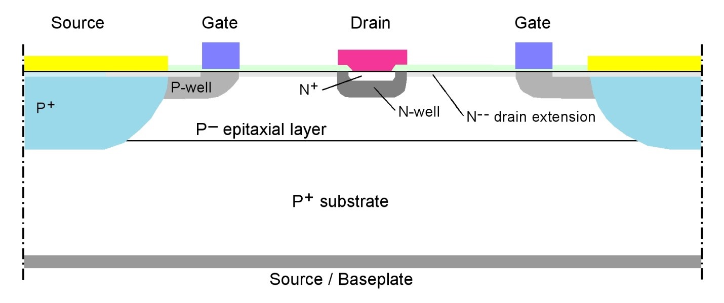
Figure 1: Simplified die structure of a Si LDMOS power transistor. LDMOS devices have multiple gate channels; two are shown here.
Key features of Si LDMOS include: high linearity, especially when compared to other silicon technologies; low input and output impedances, requiring internal matching for the desired frequency band; lower drain-gate capacitance than GaAs; higher breakdown voltage than GaAs; and low-cost silicon fabrication processes.
GaAs FET Power Devices
Gallium arsenide has characteristics that support operation up to at least 250 GHz. These include a semi-insulating substrate with a dielectric constant of approximately 12.5 and high-bulk resistivity, which makes it possible to fabricate microstrip or coplanar waveguide (CPW) structures on-chip. GaAs is radiation resistant for space applications and provides low-noise, high-linearity and very good broadband performance. Limitations include relatively poor thermal performance and modest breakdown voltage (12 to 20 V).
GaAs MESFETs (metal-semiconductor field-effect transistors) and PHEMTs (pseudomorphic high-electron mobility transistors) also require a negative supply. GaAs is a mature technology, and several transistor structures have been developed including the MESFET, used in early transistors, and MMICs (monolithic microwave integrated circuits). PHEMT (Figure 2) and HBT (heterojunction bipolar transistor) devices followed, offering a different set of advantages for low-noise, high-frequency operation, as well as reliable fabrication.
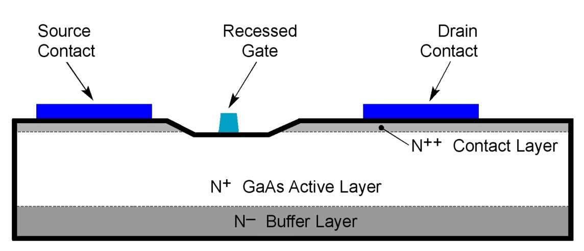
Figure 2: The basic GaAs HEMT structure.
Higher voltage GaAs devices with Vds (Vce in HBTs) breakdown voltages of 28 to 50 V and are available from a small number of manufacturers. These devices are primarily intended for satellite communication and point-to-point microwave equipment, provided in pre-matched configuration for the various microwave bands.
Key characteristics include:
|
MESFET |
Excellent microwave substrate Photonic properties (i.e., light-sensitive gate) 16 to 20 V breakdown Dual positive and negative supplies Relatively high channel temperature |
|
PHEMT |
Typical operation to 50 GHz High power and efficiency compared to other GaAs types 12 V breakdown, low operating voltage Dual positive and negative supplies E-beam fabrication increases cost |
|
HBT |
Single supply All-optical fabrication process Limited heat dissipation Requires emitter resistors for stability |
|
HV GaAs |
Reduces current requirement for GaAs amplifiers Typically available as pre-matched devices for specific bands Breakdown voltages of 28, 40, 50 are available or have been demonstrated Available using MESFET and HBT technologies Limited availability but provided by established companies |
GaN-on-SiC Technology
Figure 3 is a simplified sketch of the GaN-on-SiC die structure, depicting GaN devices fabricated using a metal-organic chemical vapor deposition (MOCVD) in a high-volume reactor on 100 mm semi-insulating 4H SiC substrates. As shown in the figure, ohmic contacts are formed directly on the top AlGaN layer, with the gate connection extended toward the drain side to create a field shaping plate.
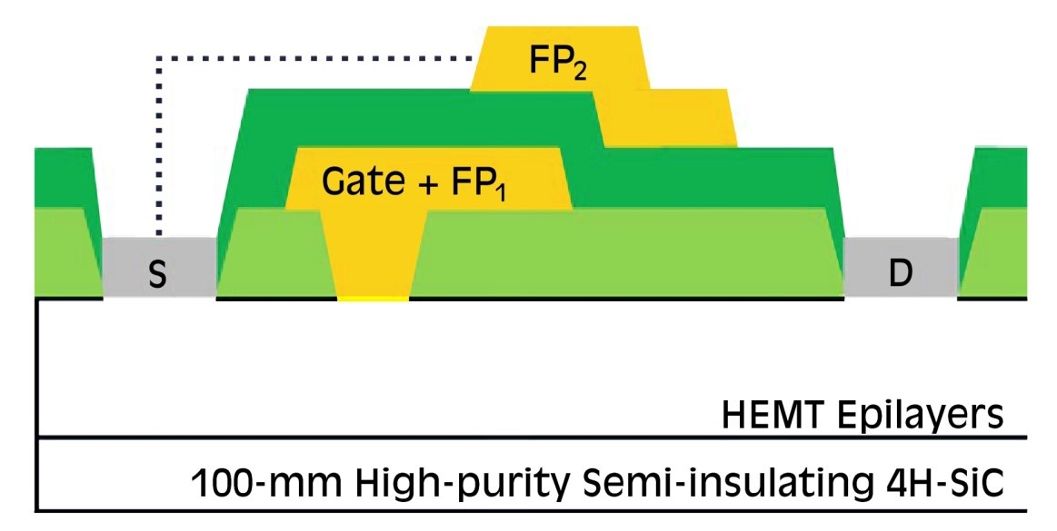
Figure 3: Schematic cross-section of the GaN HEMT RF structure.
Among power transistor technologies, GaN has a smoother transition into saturation, which means that amplifiers can operate further into the saturated region where efficiency is higher. Although GaAs and Si LDMOS also have excellent linearity, power amplifiers using GaN devices can provide the same performance with high power-added efficiency (PAE). One company reports that its new GaN-based Satcom amplifiers provide a doubling of power output for the same saturated power capability, compared to their earlier GaAs amplifiers. This behavior is achieved by several different characteristics. Compared to LDMOS or GaAs, GaN-on-SiC technology offers high electron mobility, higher breakdown voltage, higher power density, compact gate area with shorter interconnects, lower input and output capacitances, higher input and output impedances, and higher PAE.
Each of these characteristics leads to improved linearity, both within the device itself and by enabling simpler matching with wider bandwidth. With greater inherent linearity, the remaining distortion can be more easily reduced by feedback, fixed predistortion or adaptive predistortion.
Why choose a GaN HEMT device instead of an LDMOS FET or GaAsFET? Let’s take a closer look at the performance features in the list above and compare them with LDMOS and GaAs.
High electron mobility. GaN has an electron mobility approaching 2000 cm2/V·s, which is higher than LDMOS but lower than GaAs. GaAs’ higher electron mobility enhances operation at higher frequencies, however, GaN structures and processing continue to improve in the area of fmax.
Higher breakdown voltage. GaN devices are available for operation with VDS of 28 and 48 V, compared to 12 V for GaAs devices. LDMOS is available with the same operating voltages as GaN. High operating voltage results in lower drain current and lower resistive losses. Along with GaN’s internal structure, high voltage operation contributes to higher impedance and lower capacitance.
Higher power density. The GaN structure enables effective thermal conduction pathways, but the SiC substrate is also a primary contributor to high thermal performance. SiC has far better thermal performance than sapphire or silicon substrates that are also used in GaN devices. High power density allows operation at higher heat sink temperatures, simplifying cooling requirements. An obvious benefit is the safety factor for systems that are able to maintain typical operating temperatures.
Compact die size. The structure of a GaN HEMT (see Figure 3) allows straightforward implementation of passive components: thin film resistors, metal-insulator-metal (M-I-M) capacitors, and slot vias. The small size also contributes to the next characteristics in this list.
Lower input and output capacitances. Gate structure, compact size, high breakdown voltage, and straightforward interconnections all contribute to lower capacitances. AM-PM conversion, a significant distortion factor in wireless PAs, results primarily from variation in Ggs with voltage. The smaller gate periphery of GaN results in lower Cgs, less change versus voltage, and reduced AM-PM conversion than other devices.
Higher input and output impedances. Low capacitance and the higher resistive impedance resulting primarily from higher operating voltage result in higher impedances. This greatly simplifies matching, allowing simpler, lower loss circuits and enables wide bandwidth matching networks. In many cases, internal matching is not required, which is important for broadband applications. When a specific application area and frequency band is targeted, internal pre-matching can further simplify the design of matching circuitry.
Higher PAE. GaN’s slower growth in distortion as the device approaches saturation allows amplifiers to operate with less “backoff” from Psat. This behavior also supports effective implementation of linearization techniques like predistortion.
Summary
GaAs, Si, and GaN power devices all have high linearity, along with a range of characteristics that affect maximum power output, frequency range, bandwidth, thermal performance, and ease of circuit implementation. When all factors are taken into consideration, GaN has the overall highest performance for many applications, especially when a designer’s priorities include high PAE, excellent thermal performance, and easy implementation of broad bandwidth matching.


