If you think antennas must live “outside” a circuit, think again: they can also be housed in a small package adjacent to the active components they serve.
The RF signal chain has become increasingly integrated in the past years. Whether by merging RF circuitry with the digital function onto a single die or by co-locating the RF chip with one or more die for the rest of the system in a single package, much of the end product and its functionality can be provided by an IC or housed in a small module or package that resembles a large monolithic IC device.
But there are still two functions that don’t easily fit on-chip, at least not yet — the power source (almost always a battery or supercapacitor) and the antenna. While there’s no solution in sight yet for the power source, there are solutions in use now under the right circumstances for the antenna. This FAQ will look at developments and technologies which incorporate the antenna in an IC-like package and how it is done.
What is the antenna technology we are looking at?
It is called “antenna in package” (AiP) and the similar “antenna on package” (AoP). We’ll use the term AiP for both.
What is Antenna-in-Package (AiP) technology?
AiP is an antenna packaging approach that implements an antenna or antennas in an IC-like package that also houses the bare RF chip transceiver. The AiP combination can be further integrated with front-end components such as power amplifiers (PA) or low-noise amplifiers (LNA), switches, filters, and even power management integrated circuits (PMIC) using system-in-package (SiP) technologies. The AiP process makes use of packaging techniques such as double-side molding, selective molding, passive component integration, and various electromagnetic interference (EMI) shielding techniques.
What does an AiP structure look like?
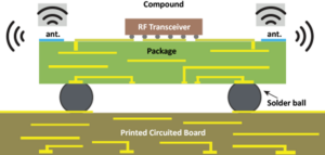
A representative design uses a flip-chip ball grid array (FCBGA) AiP and includes an RF chip (transceiver) attached to a package substrate with solder balls for connection to a main PCB, Figure 1. An antenna, or even an array of antennas, sits on top of the upper portion of the package substrate, allowing wireless communication and detection. Flip-chip techniques connect the RF chip to the substrate, thereby minimizing the interconnect loss.

Figure 1. The concept of SiP is clear enough: mount the antenna on top of the array of chips and connect it to the RF chip, then enclose the entire assembly (image: ASE).
What is the technology context for AiP?
It is a specialized variation of system-in-package (SiP) design and manufacturing technology (Figure 2).

Figure 2. Much of SiP technology derives from system-in-package advances (image: Amkor Technology).
What frequencies and wavelengths are well suited for AiP?
The answer starts with basic wavelength facts: at 1 GHz, electromagnetic wavelength (usually denoted by Greek lambda λ) is 0.3 meters; at 10 GHz, it’s 0.03 meters (3 cm/30 mm); and at 100 GHz, it’s 0.003 meters (3 mm). These wavelengths and associated antenna sizes are dimensionally compatible with AiP and IC-like package size.
For what frequencies is AiP a more-likely fit?
Due to physical wavelength issues, the best fit — but not the only one — is in the millimeter wave (MM wave or mmWave) spectrum. This is the band of the spectrum with wavelengths between 10 millimeters (30 GHz) and 1 millimeter (300 GHz), also called the extremely high frequency (EHF) band by the International Telecommunication Union (ITU). However, there is also a lot of AiP activity in the 1 to 30 GHz range.
What’s driving the implementation and adoption of AiP?
AiP technology is widely already adopted in high-frequency applications such as 60-GHz radios and gesture radars, 77-GHz automotive radars, 94-GHz phased arrays, 122-GHz imaging sensors, 300-GHz wireless links as well as 5G mobile networks operating at millimeter-wave frequencies such as 28, 39, 60, 77, 90 GHz and beyond.
Is there further impetus from 5G?
In addition to the usual quest to do more in a smaller overall product package, AiP is being driven by the 5G rollout which uses 1 to 10 GHz as well as higher frequencies.
How is the 4G to 5G transition driving, and being driven by, AiP?
In most 4G devices as well as sub-6GHz applications, antennas are manufactured in discrete form, either as a printed shape on the PCB or as a discrete antenna component to be assembled near the RF front-end chip (transceiver) with an associated matching circuit. Thanks to significantly smaller antennas at mmWave frequencies of 5G devices, the antenna in the mmWave band can be directly integrated in the package. Further, the multiple antennas needed by some 5G designs for their MIMO (multiple in/multiple out) diversity antenna arrangements are a good fit for AiP.
What are the advantages, in principle, of AiP?
Compared with placing the antenna as a separate component on or near the system PCB, the key benefits of placing the antenna and RF chip (transceiver) into one package include:
- a shorter interconnection between the antenna and the RF chip that improves signal integrity and offers reduced signal attenuation,
- reduces the range and propagation challenges that occur at higher frequencies,
- and reduces system-level certainty and design difficulty in many cases.
- The smaller overall form factor of the RF “solution” is also a competitive advantage.
What are the potential downsides of AiP?
There are several:
- it is not suitable for all RF designs, even those at frequencies above 1 GHz or even 10 GHz.
- It means that the bill of materials (BOM) now has a custom part — the AiP assembly — rather than off-the-shelf standard parts.
- It ties the OEM vendor to the selected packaging vendor since the AiP technology and manufacturing are largely defined by the capabilities of that resource.
- While AiP may seem to offer a cost advantage, it depends on the complexity of the design and the specifics to see if the up-front non-recurring engineering (NRE) design and setup charges do not outweigh the possible cost savings of the AiP or other benefits.
Are there any other issues?
Yes, it complicates the design effort in some ways since the individual RF and antenna elements cannot be modeled individually but must be modeled as a single unit.
The next part delves further into AiP technology and implementation.
Related EE World Content
Demonstrating antenna diversity, Part 1: The challenges
Demonstrating antenna diversity, Part 2: The PIFA
Demonstrating antenna diversity, Part 3: The Yagi antenna
Test methods for mmWave AiP designs bring tradeoffs
Wearable antennas target UWB frequencies
Lens antennas focus multiple wireless beams
What materials can be used to make miniature antennas?
The basics of dielectric resonator antennas
Software tool helps designers place antennas in design
5 tips for designing with embedded antennas
References and Resources
ASE, “Antenna in Package (AiP)”
Amkor Technology, “Antenna in Package (AiP) – Antenna on Package (AoP)”
Amkor Technology, “System in Package”
Chip Scale Review, “Antenna in AiP technology for 5G growth”
AnySilicon, “Understanding Antenna in Package Design”InsightSIP, “Case Study: Quad Band GSM integrated antenna”InsightSIP,“Case Study: ISP090401 2.4 GHz Transceiver Module with Integrated Antenna (Preliminary)”
InsightSIP, “ISP4250 Data Sheet”
InsightSIP, “ISP4520 Application note AN200601: LoRa Range versus PCB size and module position”
Keysight Technologies,”Millimeter Wave Antenna-in-Package Test”
Keysight Technologies,”Accelerate AiP Design Integration”
TMYTEK, “BBox™ 5G mmWave NR Beamforming Development Tool”
Wiley/King Abdullah University of Science and Technology, “Antenna-in-package Designs in Multilayered Low-temperature Co-fired Ceramic Platforms”
IEEE, “Antenna-in-Package Technology and Applications”


Tell Us What You Think!