NFC (Near Field Communication) is a standardized technology for coupling two devices in close proximity to one another (typically over a distance up to 10cm). It is already widely used in applications such as contactless ticketing in transit systems, in contactless payments cards and in access control systems. Its popularity is set to grow even more with the emergence of a new generation of smartphones and tablets equipped with the capability to implement contactless transactions – the Apple Pay mobile payments facility in the iPhone 6 smartphone is a good example (see Figure 1).
The performance requirements for these contactless transactions that device manufacturers aim to meet are stringent. Consumers expect simple operations such as opening a ticket barrier or making a card payment in a shop to just work. Users have no patience, and will not accept any delay or failure when using a contactless device.
In theory, the (many) standards governing the design, testing and operation of NFC-enabled devices are meant to ensure that the consumer experience is quick, easy and reliable.
In practice, the standards are so complex, and the potential operating environments so varied, that standards compliance on its own is very far from guaranteeing that two NFC devices will communicate as easily as the user expects them to.
In fact, any manufacturer producing a device with NFC contactless capability is highly reliant on the quality of the main NFC IC (tag or reader) that implements the NFC physical and protocol layers. As this article shows, the verification of an NFC IC’s quality calls for a highly complex and systematic testing regime. Design teams using an NFC chip would therefore do well to understand the scope and rigour of the testing to which their chosen IC has been subjected.

Fig. 1: Consumers expect a phone to implement contactless transactions instantly and reliably.
Complex Web of Standards
The purpose of standardising NFC technology (under the aegis of the independent NFC Forum) was to ensure that NFC devices can interoperate reliably.
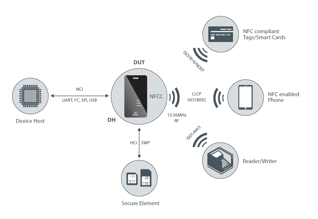
But at the time when the NFC Forum began the standardisation process, certain contactless devices, methods, protocols and use cases were already available. More use cases still continue to emerge. This makes interoperability and backwards compatibility hard to achieve. The result is that there is not a single “NFC standard,” but rather a variety of specifications maintained under the umbrella of the NFC Forum (see Figure 2).
The complexity starts at the basic hardware level with the interface to the NFC IC: SWP (single-wire protocol), UART, I2C, half-duplex serial peripheral interface and even USB have to be supported on the wired side; the RF system running at 13.56MHz provides the contactless interface.
A layer above, various communication protocols, such as NCI and HCI, are used by the Device Host and Secure Elements to communicate with the chip. ISO14443/ISO18092, ISO7816/NDEF (NFC Data Exchange Format) or LLCP (Logical Link Control Protocol) provide for communication over the RF field.
This is not all. Some NFC ICs can operate in more than one mode: Reader/Writer mode, Card Emulation mode and Peer-to-Peer mode may all be supported.
Finally every mode consists of various behaviours, roles and states (such as initiator/target, polling/listening, tag type emulation) which are intended to ensure consistent behaviour across all NFC ICs.

Fig. 2: “NFC” is an umbrella term covering multiple use cases, standards and protocols.
NFC is a highly complex standard, and this means that a deviance from any one of millions of standard specifications can cause communication between two NFC devices can fail. It is true, of course, that not all NFC ICs have to implement the complete NFC Forum specification. A Type 2 tag, for instance, would implement a much reduced subset, while an NFC controller (NFCC) in a mobile phone must support the entire set of specifications. In addition, any component of the NFC system can impair its performance if badly designed or manufactured, and OEMs must pay attention to elements such as the antenna and the power supply.
No matter what NFC functionality is required, however, the integrity and performance of the host device depends absolutely on the quality of the NFC IC. And verification of its quality calls for comprehensive testing.
What Should Be Tested?
Given the variety of protocols, modes and interfaces that an NFC IC must implement, high-level testing of the IC’s operation in a finite number of use cases will fail to adequately characterize the device. It risks:
- failing to uncover faults that could emerge in a use case or environment that has not been tested, and
- masking the location of faults, which could be at the physical layer, protocol layer or application layer.
For this reason, the correct approach is to break the test routine down into various subsets. The first such subset is the low level protocols. In protocol testing, the goal is to verify the operation of specific aspects of the protocol, such as the semantics, syntax or timing. This checks the integrity of the the basic communication system.
At the next level are behavioural tests. Here, the effect of commands and responses on the system can be checked. Using a given command set, the tests should implement state transitions: the test engineer can discover whether the device ended up in the correct state by analysing the received response. In the new state, the system should respond differently to external stimulation than in the previous state.
Last but not least is interoperability testing. Some NFC chips have repeatedly encountered interoperability failures, even though devices may be compliant with the NFC standards.
Exhaustive testing has revealed that the root of the problem often lies with the timing constraints: these are very tight, and NFC devices are sometimes unable to meet these constraints in certain use cases. Drawing on the results of its interoperability tests, companies can modify their devices to tighten their own timing windows, while relaxing the timing windows applied to the device (see Figure 3).

Fig. 3: High-performance analogue circuitry gives other devices more time in which to respond to NFC signals.
The benefit of implementing such a thorough programme of low-level device testing is that, if the IC passes all the tests, the manufacturer can assume that all verified higher-layer applications will work on it. For instance, a use case such as PHDC (Personal Health Device Communication, for certain forms of data exchange) takes place on a protocol layer that has already been verified, so if the operation of PHDC itself is verified, the entire system be assumed to be verified.
For the sake of completeness and integrity, of course, it makes sense to run tests for use cases such as PHDC on the actual NFC stack.
Implementing an appropriate test environment
The description of the test requirements above shows that testing an NFC IC is a complex task which imposes a requirement for considerable hardware, software and human resources. In brief, the key elements of an appropriate test environment are:
- the capability to access the source code repository which is used by the developers to get the latest version of the implementation. A mechanism must also be in place to update the firmware on the device under test via a debugger or boot loader before the actual test run is started;
- the capability to interact with the device on all its interfaces simultaneously, which calls for concurrent communicationl;
- integrated third-party test suites. Certification runs require the use of approved third-party test suites. It is useful to have the ability to do pre-runs at the lab, to be able to detect failures early and to fix them. This reduces the need for real certification runs, thus saving time and money;
- for the software development teams, it is important to be able to run tests manually at their desks, so as to support debugging by reproducing fails. This also allows them to test code changes before integrating them into the repository. To speed up this regression testing, any subset or combination of tests should be executable; and
- logging capability is an important part of a test bench. During development, the developer must be able to reproduce a fail which might have occurred during overnight testing. Comprehensive logging provides information that enables the developer to locate and identify a fail.
Analysis of the results of automated test runs is provided by the test system itself. It provides a graphical representation of test runs, so that the developer can easily see the total number of executed tests, the number of passes and fails, and the history, which shows trends.
The Value of a Verified NFC IC
The resources and technology ploughed into NFC IC testing are of great benefit to OEMs that make NFC-enabled devices: the use of a guaranteed high-quality NFC IC makes it easier for a product manufacturer to create an NFC device that consumers will find quick, easy and reliable.
Of course, the NFC IC will only be one of many parts embedded in the end product, so testing of the entire system will always be necessary. But depending on the configuration of the NFC sub-system (for instance, as an NFC reader or NFC tag), certain scenarios and use cases can be defined and tested while others can be assumed to be properly operational. For instance, there is no need for the end product manufacturer to test error handling at the protocol level, provided it has been tested thoroughly at the sub-system level.
But for end-to-end tests of the NFC sub-system embedded in an end product, it is again necessary to have access to the inputs and outputs of the system, that is, to the part which interacts with the device host on the one side as well as its counterpart on the RF side, such as a credit card or phone.
In fact, the nature of the host product manufacturer’s end-to-end tests depends on the use case for which the product is intended. But one thing is certain: standards compliance and high system performance can only be guaranteed if the product uses NFC components that have themselves been rigorously and thoroughly verified.


