The use of mmWave technology is growing across various applications, from 5G telephony to automotive systems and drones. At mmWave frequencies, signal integrity (SI) is a major concern. SI measures the signal’s ability to propagate without distortion or undue losses. It measures the quality, or distortion, of the signal passing through the printed circuit board (PCB) traces, cables, and connectors in a system. Signal distortion can be disruptive and even destructive to reliable system operation and happens due to factors like impedance mismatches, reflections, ringing, crosstalk, jitter, ground bounce, etc.
SI optimization takes different forms depending on the signal modulation scheme used as well as other factors. For example, the need to control ringing is critical for signals that use ASK, PSK, QAM, QPSK, or any other signal modulation scheme that uses sudden changes in phase or amplitude to encode digital information. For FSK and other frequency modulation schemes that are sufficiently smooth, the impact of ringing is less. Ringing is only one aspect of SI. Other SI and PCB layout considerations include:
- Controlling impedances ensures that signal lines have matched source and receiver impedances that are the same as the impedance of the signal lines themselves.
- Impedance discontinuities need to be managed and minimized and can occur at vias in a signal path, branches in signal paths, line stubs, when signal lines are mated to connector pins, and when the signal lines start at the source and/or end at the receiver.
- Propagation delays can be minimized by trace length matching.
- Crosstalk noise can be controlled by increasing the spacing between adjacent signal traces, using a lower dielectric constant substrate material, using differential signaling with tightly coupled differential pairs, and ensuring that the signal return paths are as wide and uniform as possible.
- Power and ground distribution issues (including ground bounce) can be addressed using a number of design approaches, including placing decoupling capacitors as close as possible to device power and ground pins and placing the power and ground planes close together and near the surface of the PCB to reduce via inductances.
Controlling impedance is the single most important factor in preventing SI issues in mmWave PCBs. Interconnect geometries are important in determining and controlling impedance. Trace geometry is a complex factor and includes losses from dielectric absorption, skin effects, roughness losses, and scattering in addition to adequate isolation.
High-frequency PCBs often rely on microstrip or stripline transmission line geometries with guard vias to isolate different circuit blocks and reduce radiated emissions. An alternative approach is using grounded coplanar waveguide (GCPW) routing, which can provide much lower losses and stronger isolation compared with the other two routing approaches, especially on a surface layer.
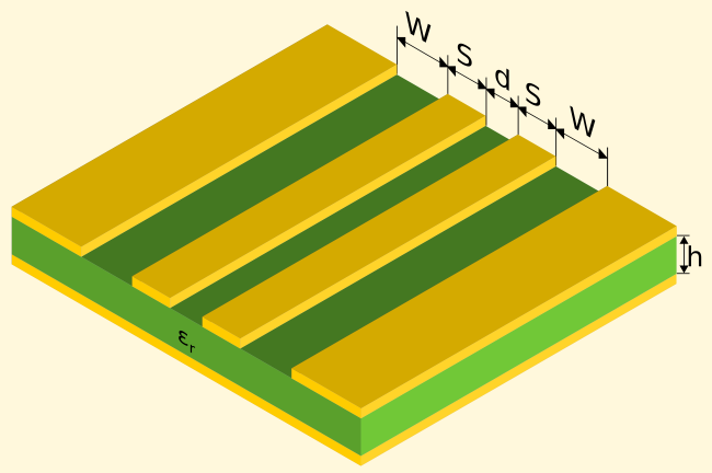
Example of edge coupled grounded coplanar waveguide (GCPW) in a PCB layout for mmWave frequencies. (Image: Northwest Engineering Solutions)
With GCPWs, the skin effect is still there, but the ground planes surrounding the GCPWs draw the currents to the waveguide’s horizontal edges, where the surface roughness is the lowest, thereby reducing the skin effect. The use of GCPWs versus microstrips and striplines is dependent on the loss tangent of the substrate at the frequency being used. At mmWave frequencies, GCPWs are often preferred with FR4 substrates, while microstrips and striplines are used with other substrate materials.
Dielectric absorption in the substrate is only one factor in losses. Copper roughness and skin effects are also important considerations. At mmWave frequencies, current is confined near the edge of conductors, creating the skin effect. Rough surfaces of etched copper are also a source of dc losses. Instead of using etching, the use of additive processes to create traces on a substrate can reduce roughness and improved efficiency at high frequencies.
Traditional subtractive PCB manufacturing processes create traces with a trapezoidal cross section with the top narrower than the bottom. The trapezoidal cross section angle can be 25 to 45 degrees off the vertical, modifying the impedances of the traces and reducing performance at mmWave frequencies. In addition to reducing surface roughness, the use of additive PCB fabrication processes results in vertical sides on traces, eliminating the limits that a trapezoidal cross section places on high-frequency performance.
Coax cables for RF and mmWave
Basic coaxial (coax) cable is a two-conductor structure with a center conductor and an outer conductor, which also acts as a shield with an insulating spacer between the two. The structure provides tight control over the cable impedance and results in improved performance at high frequencies. Coax cables are used in a variety of applications. The two primary types of coax are 50 Ω which is used for high-speed data, RF, mmWave transmissions, and 75 Ω, used primarily in video signal and other applications.
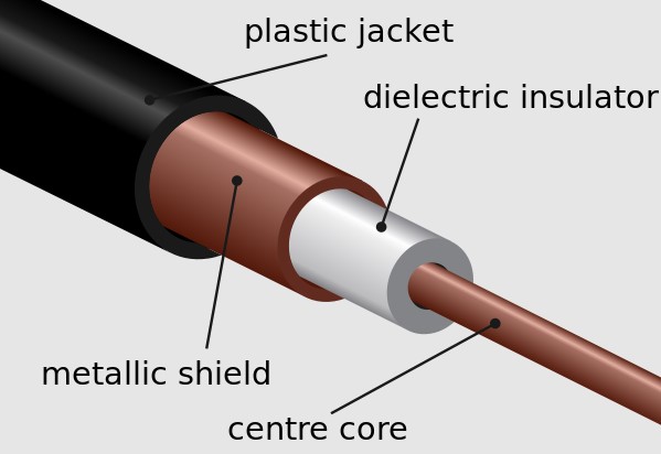
Basic coaxial cable construction with a single shield. (Image: Wikipedia)
High-performance coax cables have been developed for noisy environments. These cables can consist of 10 or more elements (see diagram below):
- Center conductor – primary conductor, often made from copper-clad steel.
- Center conductor bond – polymer coating to block moisture migration.
- Dielectric – low loss, low density, polyethylene foam.
- First outer conductor – tape shield of aluminum-polymer-aluminum.
- Second outer conductor – aluminum-polymer-aluminum tape is used in tri-shield and quad-shield cables to provide the increased high frequency (HF) shielding and isolation.
- Third outer conductor – also an aluminum-polymer-aluminum tape to further enhance shielding and mechanical integrity.
- Fourth outer conductor – to enhance low-frequency shield isolation in extreme RF noise environments, a 34 or 36 AWG aluminum braid is added.
- Corrosion-resistant protective coating.
- Jacket – a UV stable outer coating covers the entire assembly to protect the core during installation and for the installed life of the cable.
- Integral messenger (optional) – support member made with a galvanized, carbon steel wire to provide additional mechanical strength.
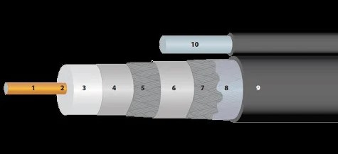
High-performance coax can have multiple layers of shielding for protection in noisy environments. (Image: PPC Broadband)
mmWave connector and cable compromises
As noted above, the primary impedance for coax transmission lines and connectors is 50 Ω in the U.S. It represents a performance compromise: 77.5 Ω is the theoretical impedance for minimum attenuation, and 30 Ω is the theoretical impedance for maximum power transfer. The average of those two impedances is 53.75 Ω and is rounded off to 50 Ω, which provides a good compromise between minimum attenuation and maximum power transfer. There are connectors available with other impedances, the next most popular impedance being 75 Ω (for minimum attenuation performance). Because it provides superior attenuation performance, 75 Ω is in fairly wide use internationally and long line communication systems.
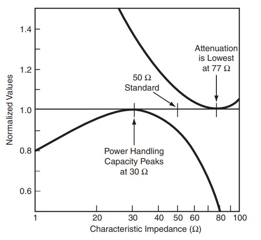
Coaxial transmission line and connector power handling versus attenuation tradeoff. (Image: Maury Microwave Corp.)
The diameter of coax connectors and cables needs to be much smaller than the signal wavelength. Otherwise, a phenomenon called “moding” occurs. Moding refers to an unwanted waveguide mode (non-transverse electromagnetic mode, or TEM) that appears when the connector is being driven past Fcutoff (see image below). Moding is why 2.92 mm RF connectors are good to 40 GHz, 2.4mm connectors to 50 GHz, and 1.85 mm connectors to 67 GHz. Moding sets physical size limitations on coax cable. The dominant loss mechanism in the coax cable is the diameter of the center conductor. But if the center conductor’s diameter is larger, the outer diameter grows too, and cutoff frequency drops. This is why cable manufacturers are producing foamed dielectrics: it reduces the shield diameter “D” for a given center conductor diameter “d”.

To avoid undesired transmission modes, coax connectors need to be sized to the correct cutoff frequency (Fcutoff). (Image: Samtec)
mmWave connector standards
There are several IEEE standards related to mmWave connectors, including:
- IEEE P287 – Standard for Precision Coaxial Connectors (DC-110 GHz) – This standard specifies coaxial connectors for precision electrical measurements to 110 GHz. The frequency range of the standard is increased from 65 GHz to 110 GHz since in the market exists a 1 mm connector with a rated upper minimum operating frequency of 110 GHz.
- IEEE P287.1 – Standard for Precision Coaxial Connectors at RF, Microwave and Millimeter-wave Frequencies. Part 1: General requirements, definitions, and detailed Specifications – This standard specifies coaxial connectors for precision electrical measurements for RF, microwave, and millimeter-wave frequencies.
- IEEE P287.2 – Recommended Practice for Precision Coaxial Connectors at RF, Microwave and Millimeter-wave Frequencies – Part 2: Test Procedures – This recommended practice specifies the mechanical and electrical test procedures to be used for precision coaxial connectors used at RF, microwave, and millimeter-wave frequencies.
- IEEE 287-2007 – IEEE Standard for Precision Coaxial Connectors (DC to 110 GHz) – This standard presents minimum performance requirements to standardize both hermaphroditic and pin- and socket-type connectors. It includes recommended electrical and mechanical test procedures for general and laboratory precision connectors.
Summary
SI is an important factor in the design of mmWave PCB and interconnect systems. It measures the quality, distortion, and signal passing through the PCB traces, cables, and connectors in a system. Signal distortion can be disruptive and even destructive to reliable system operation and happens due to factors like impedance mismatches, reflections, ringing, crosstalk, jitter, ground bounce, etc. As shown, there are several tools that designers have to optimize SI in mmWave applications.
References:
9 Factors That Lead to Signal Integrity Issues in a PCB, Sierra Circuits
Computing the differential impedance of an edge-coupled coplanar waveguide with ground, Electronics Stack Exchange
How will 5G affect your PCB design?, Proto-Electronics
Recommended Practice for Precision Coaxial Connectors at RF, Microwave and Millimeter-wave Frequencies, IEEE
RF PCB Layout: mmWave Routing and Interconnect Losses, Northwest Engineering Solutions
Waveguides, Modes, and Cutoff Frequencies, Samtec


Tell Us What You Think!