5G Technology World

  • 5G Technology and Engineering
  • FAQs
  • Apps
  • Devices
  • IoT
  • RF
  • Radar
  • Wireless Design
  • Learn
    • 5G Videos
    • Ebooks
    • EE Training Days
    • FAQs
    • Learning Center
    • Tech Toolboxes
    • Webinars/Digital Events
  • Handbooks
    • 2024
    • 2023
    • 2022
    • 2021
  • Resources
    • Design Guide Library
    • EE World Digital Issues
    • Engineering Diversity & Inclusion
    • Engineering Training Days
    • LEAP Awards
  • Advertise
  • Subscribe

Timing IC combines functions for Open RAN

By Martin Rowe | August 6, 2021

Microchip’s ZL30735 integrates eight DPLLs, five low-output jitter synthesizers, and an IEEE 1588-2008 protocol stack.

The splitting of radio access network functions creates an Open RAN that promises greater innovation and features in 5G networks. Splitting the traditional baseband unit into radio units (RU), distribution units (DU) and centralized units (CU) brings timing issues not present in an integrated RAN. Microship Technology addresses those issues with a series of timing ICs.

In Meet timing requirements in 5G networks Microchip’s Jim Olsen notes “the BBU is no longer a timing interface or demarcation point in 5G networks because it’s disaggregated into the Centralized Unit (CU) and Distributed Unit (DU) functional blocks in an Open RAN architecture.”

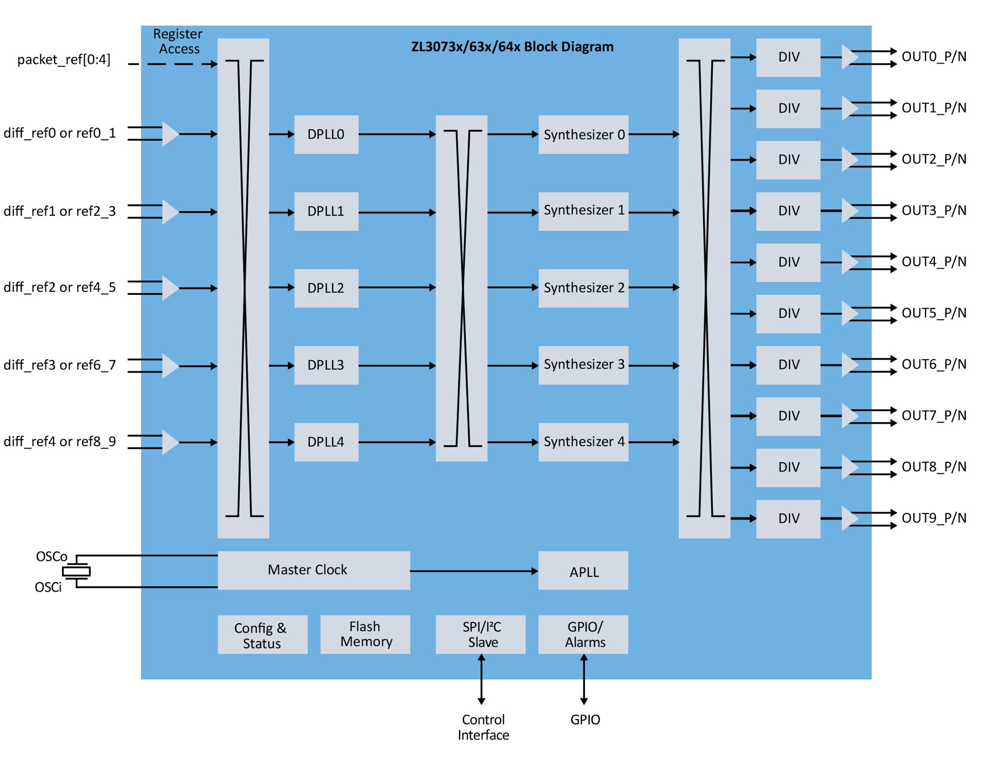
The latest addition to Microchip’s timing family, the ZL30735, combines eight independent DPLLs, five extremely low-output jitter synthesizers, and an IEEE 1588-2008 Precision Time Protocol Stack and Synchronization Algorithm software modules.

Microchip’s measure, calibrate and tune capabilities let 5G networks comply with International Telecommunication Union – Telecommunication (ITU-T) Standard G.8273.2 Class C (30 ns max|TE|) and the emerging Class D (5 ns max|TEL|) time error requirements. It also supports compliance for ITU-T G.8262, G.8262.1, G.813, G.812, Telcordia GR-1244, GR-253 and packet-timing compliance with ITU-T G.8261, G.8263, G.8273.2 (class A,B,C,D), G.8273.4.

The ZL30735 has five GPIO pins and an SPI or I2C processor Interface. It operates at VDD core voltages of 1.8 V and 3.3 V.


Filed Under: 5G, Industry Standards, OpenRAN, Oscillators, Timing
Tagged With: microchip
 

Next Article

← Previous Article
Next Article →

Related Articles Read More >

Mixed-Signal Devices clock oscillator
Oscillators generate clocks through digital techniques
circuit board timing
How timing and synchronization improve 5G spectrum efficiency
Timing module extends the life of legacy network equipment
What are 5G’s, the different types, and how are they used?

Featured Contributions

  • Overcome Open RAN test and certification challenges
  • Wireless engineers need AI to build networks
  • Why AI chips need PCIe 7.0 IP interconnects
  • circuit board timing How timing and synchronization improve 5G spectrum efficiency
  • Wi-Fi 7 and 5G for FWA need testing
More Featured Contributions

EE TECH TOOLBOX

“ee
Tech Toolbox: 5G Technology
This Tech Toolbox covers the basics of 5G technology plus a story about how engineers designed and built a prototype DSL router mostly from old cellphone parts. Download this first 5G/wired/wireless communications Tech Toolbox to learn more!

EE LEARNING CENTER

EE Learning Center
“5g
EXPAND YOUR KNOWLEDGE AND STAY CONNECTED
Get the latest info on technologies, tools and strategies for EE professionals.

Engineering Training Days

engineering
“bills
5G Technology World
  • Enews Signup
  • EE World Online
  • DesignFast
  • EDABoard Forums
  • Electro-Tech-Online Forums
  • Microcontroller Tips
  • Analogic Tips
  • Connector Tips
  • Engineer’s Garage
  • EV Engineering
  • Power Electronic Tips
  • Sensor Tips
  • Test and Measurement Tips
  • About Us
  • Contact Us
  • Advertise

Copyright © 2025 WTWH Media LLC. All Rights Reserved. The material on this site may not be reproduced, distributed, transmitted, cached or otherwise used, except with the prior written permission of WTWH Media
Privacy Policy

Search 5G Technology World