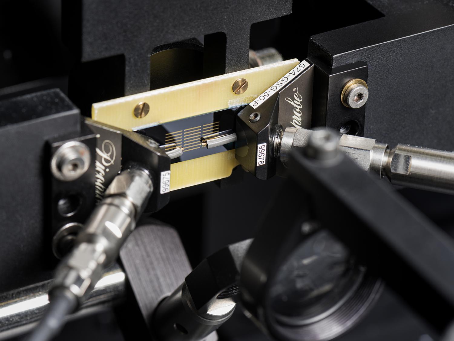
Part of the experimental setup for laser-based vector network analysis. A cluster of planar waveguides has been fabricated on a semiconductor. The waveguides are contacted at either end using two microwave probes. A laser beam is focused from the front onto the waveguide and generates in a photoconductive gap ultrashort voltage pulses. The voltage pulses are detected by a second laser beam which is focused from the back through the substrate onto the planar waveguide. (Credit: PTB)
Vector network analyzers (VNA) are among the most precise high-frequency measurement devices available today. Due to continuous development within the last decades VNAs are usable up to frequencies of 1 terahertz (1012 Hz) and complex error correction algorithms exist. However, VNAs are very expensive and require multiple frequency extenders in order to cover a wide frequency range. At the Physikalisch-Technische Bundesanstalt (PTB) a VNA has been developed which utilizes optoelectronic techniques based on femtosecond lasers. Such devices constitute a cost-effective alternative to conventional VNAs and might be used for high-frequency measurements in the future. The results have been published in the present issue of the renowned journal IEEE Transactions on Microwave Theory and Techniques.
The measurement principle of VNAs relies on the detection of power waves at discrete frequencies. Variation of the frequency allows frequency-resolved measurements. The measurement results are typically specified in terms of scattering parameters. In order to characterize a high-frequency device accurately, forward and backward propagating signals have to be separated, which is accomplished using directional couplers.
At PTB, researchers have shown that frequency-resolved scattering parameter measurements can also be realized using laser-based measurement techniques. For this purpose, a femtosecond laser emitting pulses approximately 100 femtoseconds (10-13 s) long in the near infrared is utilized. The laser beam is divided into a pump beam and a probe beam. The pump beam excites a so-called photoconductive switch integrated in a planar waveguide. This excitation leads to voltage pulses approximately 2 picoseconds long propagating on the planar waveguide. The probe beam is used to detect the electric field of the voltage pulses, employing the Pockels effect of the substrate on which the planar waveguide is fabricated. By changing the time delay between pump and probe beam through the use of a delay line, the shape of the voltage pulse can be accurately measured.
As main innovation, the PTB researchers have developed a laser-based measurement method allowing the separation of forward and backward propagating signals on the planar waveguide. This technique is the equivalent of directional couplers used in conventional VNAs. The separation, which requires the detection of voltage pulses at different positions on the planar waveguide, even works in the case of temporally overlapping forward and backward propagating signals. With the new optoelectronic time-domain measurement method, scattering parameter measurements on planar waveguides up to 500 GHz with a 500 MHz frequency spacing have been demonstrated. The method can also be utilized for the characterization of coaxial high-frequency devices and for the realization of a very precise voltage pulse standard.


