By Francesco Di Domenico, Principal Application Engineering at Infineon Technologies
As cellular network operators begin to switch on and deliver the 5G experience, the world awaits with mounting anticipation of the benefits the new mobile network technology will bring. Consumers can expect higher bandwidth, lower latency and more advanced service delivery from 5G, but it comes with a cost, of course. To the customer, this will be an incremental price rise in line with the services offered, but for the carriers and network operators it will be almost exponential; a short-term pain for long-term gain.
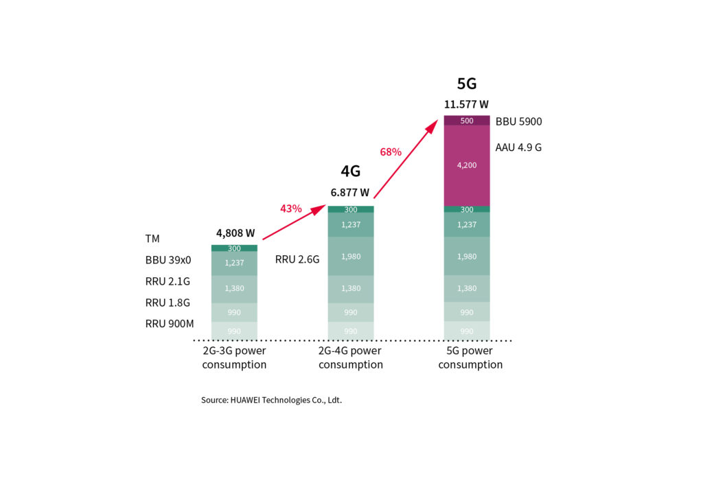
As well as the cost of new equipment, operational expenditure is also set to rise, because there is no escaping the fact that 5G will require more power than 4G, much more; industry estimates predict an almost 70 percent increase in power requirements (Figure 1). As an example, a 4G base station consumes around 7 kW of power, while a 5G base station will need in excess of 11 kW. For a site that carries multiple channels, this could reach 20 kW.
5G Connectivity is power-hungry
While the efficiency of 5G will see a reduction in Watts per bit, the network’s greater capacity will result in a net increase in total power consumed. One reason for this is the topology of the network; the use of Massively Multiple-In, Multiple-Out (MIMO) antennas will see an equally massive increase in the number of transceivers used. The terminology used here is 64T64R, or 64 transmit and 64 receive; compare that with a 4G base station that typically used 4T4R and it becomes clear where the extra power is being applied.
In fact, it seems that some operators are considering reducing the number of transceivers, and therefore network capacity, to 32T32R or even 16T16R, as a way of mitigating the increased power requirements. This is, in part, because of the challenges involved with delivering more power.
It is well reported that 5G will require more base stations than previous networks, largely because greater bandwidth requires greater capacity, but also because the wavelengths used in 5G have shorter propagation distances. This will require putting base stations in new locations and in order to provide a wide level of coverage, this will include sites in both populous urban areas as well as rural and remote locations. In both cases, the cost of physically accessing power will be considerable, pushing up the operational costs.
Compounding this is the fact that the industry has standardized on 3 kW 48 VDC power supplies. As the total power requirements will at least double, operators will need to increase the power density significantly in order to deliver more power in the same footprint using predominantly the same infrastructure, including cabling.
Power at the Edge
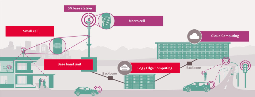
The new 5G networks will require greater capacity at every point, but this is likely to be most apparent at the edge (Figure 2). While there are equivalences in the existing network, they are likely to be power-restricted, with just enough power available to operate the 4G cells. Delivering twice the amount of power to these stations may very well be untenable, either because the provider’s infrastructure is simply unable to support the increased power, or because the cost of doing so makes it commercially impossible.
The reason for this increased demand for power isn’t solely due to the extra hardware needed to implement 5G; it will also be a result of the increased functionality of the stations. The services offered by 5G will surpass previous networks in every way, and this will require additional compute power.
GaN in 5G
The only way to address this design challenge is to increase the efficiency of the power conversion stage, thereby delivering greater power output in the same footprint, without the commensurate 70 percent increase in input power. Two technologies are making this possible; GaN and SMD packaging.
Firstly, SMD, or surface-mount device packaging, provides a smaller footprint for integrated devices. More significantly, and as the name suggests, these devices are mounted on the surface of a PCB, as opposed to through-hole devices (THDs), which are mounted through the PCB using plated through-holes and legs. In general, SMD provides an instant increase in function density, as SMD packages are smaller than their THD counterparts. However, in terms of power semiconductors, moving from THD to SMD without addressing the efficiency of the device will result in a higher heat density.
Heat density is the other face of power density and while it is essential to increase power density, it is only feasible if heat density remains the same or, preferably, goes down.
The use of SMD packaging allows for simpler PCB design, not least because it allows for the use of top-side cooling. This involves putting the top of the power component in direct contact with the enclosure, typically aluminum, which creates a much shorter thermal path from the transistor’s junction to ambient air.
Adopting SMD with conventional silicon-based power semiconductors will increase power density but it will also increase heat density. Even with better thermal conductivity, the device will still be constrained by the operating temperature unless switching efficiency also increases. Power conversion topologies based on MOSFETs have reached efficiency levels in the region of 98 percent, leaving little headroom for further improvement. However, power transistors based on wide bandgap technologies such as silicon carbide (SiC) and gallium nitride (GaN) are inherently more efficient than MOSFETs, which makes them the perfect complement to SMD packaging.
More significantly, GaN in SMD has physical properties that make it better than silicon at switching high power at high frequencies. This includes a lower on-resistance but, perhaps more importantly, it has significantly lower switching losses, which allows the power converter to operate at higher switching frequencies. This has the direct benefit of simplifying the magnetic discrete components needed to support a switching power supply topology. This, in turn, results in an overall smaller solution and, consequently, higher power density. Most importantly, the higher efficiencies inherent with GaN means heat density does not increase and, in most cases, goes down.
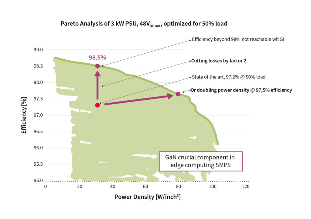
The graph shown in Figure 3 applies Pareto Analysis to plot in two dimensions all possible combinations of a 3kW/48V PSU, in terms of power density and efficiency at 50% load. As this demonstrates, using CoolGaN in power conversion could result in either higher efficiency, greater power density or a combination of both, compared to even the most state-of-the-art silicon MOSFET solutions.
Conclusion
GaN is a technology supremely suited to power conversion in 5G network infrastructure. The application’s requirements almost exactly match the technology’s benefits and while there is really no such thing as too much power capacity, delivering the right amount in the right places will enable 5G to deliver on its promise.
The increased power requirements of 5G over 4G will put pressure on the existing infrastructure and force manufacturers to innovate in order to increase power density and reduce heat density while improving power efficiency. To learn more about how Infineon’s GaN portfolio and solutions, including those in SMD, can address these challenges, please visit www.infineon.com/gan.


Tell Us What You Think!