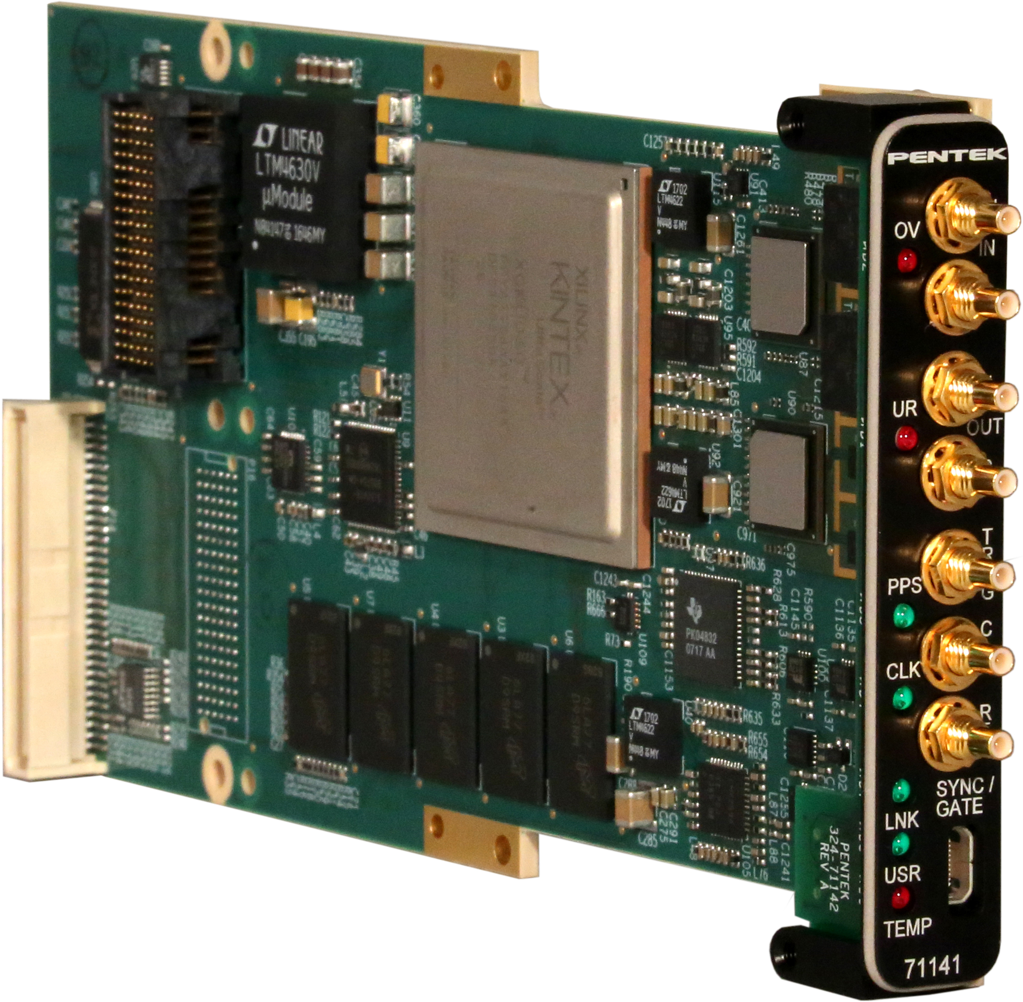
Pentek, Inc., introduced the latest member of the Jade™ family of high-performance data converter XMC modules based on the Xilinx Kintex Ultrascale FPGA. The Model 71141 is a 6.4 GHz dual channel analog-to-digital and digital-to-analog converter with programmable DDCs (digital downconverters) and DUCs (digital upconverters).
The Model 71141 is suitable for connection to IF or RF signals for very wideband communications or radar system applications including:
• Satellite communications (SATCOM)
• Phased array radar, SIGINT and ELINT
• Synthetic aperture radar (SAR)
• Time-of-flight and LIDAR distance measurement
• RF sampling software defined radio (SDR)
For applications that require unique functions, users can install custom IP for specialized data processing tasks. Pentek’s Navigator™ FPGA Design Kit includes source code for all factory-installed IP modules. Developers can integrate their own IP with the Pentek functions or use the Navigator kit to completely replace the Pentek IP with their own.
Design Saves Costs and Development Time
The Pentek Navigator tools reduce the development time and cost associated with complex designs. Users can also select the size of the FPGA they would like installed so they are getting exactly what they need performance-wise without paying for a larger FPGA they may not need. Unlike others in the industry, Pentek still provides application support to customers at no cost.
A/D Stage and Digital Downconverter
The Model 71141 is the first of the Pentek Jade products to use the Texas Instruments ADC12DJ3200 12-bit A/D. The front end accepts analog RF inputs on a pair of front panel SSMC connectors. The converter operates in single-channel interleaved mode with a sampling rate of 6.4 GS/sec and an input bandwidth of 7.9 GHz; or, in dual-channel mode with a sampling rate of 3.2 GS/sec and input bandwidth of 8.1 GHz.
The A/D built-in digital down converters support 2x decimation in real output mode and 4x, 8x or 16x decimation in complex output mode. The A/D digital outputs are delivered into the FPGA for signal processing, data capture or for routing to other module resources.
Digital Upconverter and D/A Stage
A Texas Instruments DAC38RF82 D/A with DUC accepts a baseband real or complex data stream from the FPGA and provides that input to the upconversion, interpolation and dual D/A stages. When operating as a DUC, it interpolates and translates real or complex baseband input signals. It delivers real or quadrature (I+Q) analog outputs to the dual 14-bit D/A converter. The two 6.4 GS/sec 14-bit D/As pair well with the dual input channels while delivering more than twice the output performance of previous generations of Pentek products.
Performance IP Cores
The 71141 factory-installed functions include two A/D acquisition and two D/A waveform generation IP modules. In addition, IP modules for DDR4 SDRAM memories, a controller for all data clocking and synchronization functions, a test signal generator and a PCIe Gen.3 interface complete the factory-installed functions. System integrators get to market with less time and risk, because the 71141 delivers a complete turnkey solution without the need to develop any FPGA IP.
The Jade Architecture
The Pentek Jade Architecture is based on the Xilinx Kintex UltraScale FPGA, which raises the digital signal processing (DSP) performance by over 50% with equally impressive reductions in cost, power dissipation and weight. As the central feature of the Jade Architecture, the FPGA has access to all data and control paths, enabling factory-installed functions including datamultiplexing, channel selection, data packing, gating, triggering and memory control. A 5 GB bank of DDR4 SDRAM is available to the FPGA for custom applications. The x8 PCIe Gen 3 link can sustain 6.4 GB/s data transfers to system memory. Eight additional gigabit serial lanes and LVDS general-purpose I/O lines are available for custom solutions.
Navigator Design Suite for Streamlined IP Development
Pentek’s Navigator™ Design Suite was developed from the ground up to work with Pentek’s Jade architecture and Xilinx’s Vivado Design Suite® providing an unparalleled plug-and-play solution to the complex task of IP and control software creation and compatibility. The Navigator Design Suite consists of two components: Navigator FDK (FPGA Design Kit) for integrating custom IP into Pentek sourced designs and Navigator BSP (Board Support Package) for creating host applications. Users can work efficiently at the API level for software development and with an intuitive graphical interface for IP design. The Navigator BSP is available for Windows and Linux operating systems.
Pre-Configured SPARK System Ready for Immediate Use
With a Pentek 8266 SPARK® PC, 8264 SPARK 6U VPX, or 8267 SPARK 3U VPX development system, work can begin immediately on applications. A SPARK system saves engineers time and expense associated with building and testing a development system and ensures optimum performance of Pentek boards. SPARK development systems are ready for immediate operation with software and hardware installed. In many applications, the SPARK development system can become the final deployed application platform.
Form Factors
The Model 71141 XMC module is designed to operate with a wide range of carrier boards in PCIe, 3U and 6U VPX, AMC, and 3U and 6U CompactPCI form factors, with versions for both commercial and rugged environments.
Pricing and Availability
Designed for air-cooled, conduction-cooled and rugged operating environments, the Model 71141 XMC module with 5 GB of DDR4 SDRAM is now available. Additional FPGA options are also available. The Navigator Design Suite consists of two packages, the Navigator BSP and the Navigator FDK. Delivery is 12 weeks ARO. For the latest pricing and availability information, please contact Mario Schiavone by phone at (201) 818-5900 ext.229.


