Designing an antenna into a wireless embedded or IoT device requires special care to maximize performance.
When designing a wireless device, pay attention to the antenna placement on a PCB. Space on the PCB, position, clearance, the ground plane, and correct connection to other components all affect antenna performance. Getting these aspects correct from the initial design concept will help to achieve a successful launch with reliable wireless performance.
An antenna that performs well in free space as outlined in the manufacturer’s datasheet may perform differently when installed in a device. In the worst case, an antenna squeezed into a space towards the end of the design phase without consideration of the manufacturer’s intended layout guidance will probably function poorly. The design will need a revision, which adds cost and lengthens time to market. Follow these five basic principles of designing an embedded antenna into an electronic device and get a design right the first time.
Antenna placement
Because an antenna is sensitive to its surroundings, the general position of the antenna within the device can help or hinder a design. Place the antenna in a location that protects it from objects that might cause electrical interference with the antenna.
The human body absorbs RF energy. If you are designing a wearable device that will be used on or close to the body, you may need to place the antenna on the side of the device facing away from the body. This is one reason why RF design companies conduct tests with phantom heads, bodies, and hands in anechoic chambers [Ref. 1]. Such tests reveal how well the device operates close to a person or in a person’s hand (Figure 1).

Figure 1. A phantom head in an anechoic chamber lets you test antenna performance in a controlled environment.
Similarly, metal objects close to an antenna can affect its performance. Take the case of a tracking device for bicycles. The tracker will probably be fixed to the bike’s metal frame. When a device is used against a metal object, you should place the antenna as far away from the metal structure as possible. Doing so lets the antenna radiate without interference from the metal object.
A device’s outer casing can play a role in how the antenna performs. If the case is made of metal or glass filled plastics, it can also inhibit the antenna’s radiated energy. Consider making the case from non-glass filled plastic unless you use a special antenna.
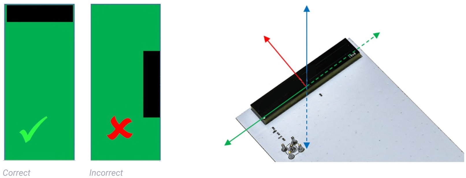
An antenna’s position on a PCB can affect RF performance. Antennas need to radiate in six directions. Figure 2 shows how placing an antenna can radiate energy in more directions when placed correctly on a PCB. Fig. 2 also shows how a position on the corner of the PCB is better because fewer of the antenna’s fields will be obstructed, and the antenna’s performance improves compared to other locations.
Antennas are often designed to operate in a corner position, but some antennas work best on a PCB’s long or short edge. Some antennas have right and left variants. You have options and thus you can select an antenna that best suits the PCB’s design and layout. You may have some freedom to vary the exact position of the antenna but study the manufacturer’s datasheet and position the antenna as recommended. This lets the antenna radiate correctly and achieve optimum performance.
Position the antenna in relation to other components
Even a high-performing antenna with good efficiency will not operate properly when close to another component that causes interference. Such interference might come from something on the PCB or another object close to the antenna.
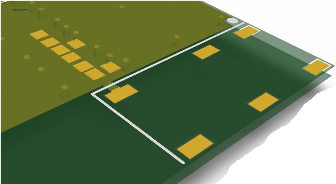
Some components cause interference in the radiated signal coming from an antenna. Batteries, LCDs, motors, and other metal objects can create noise or reflections that interfere with the antenna’s performance. Thus, you should keep the antenna as far away from these objects as possible. Figure 3 shows the antenna’s footprint and clearance through all the layers of the PCB.
Other nearly antennas can cause problems, especially if they operate at similar frequencies or harmonic resonances of the primary wavelengths. They may cause an antenna to detune. Ideally antennas should be isolated from each other, say up to -10 dB at 1 GHz and -20 dB at 2 GHz.
The antenna may also need clearance. In this area, only the antenna pads and connections to the feed are present, letting it function correctly in free space. Check the datasheet for manufacturer’s clearance specifications and measurements. The area of clearance may be a little larger than the actual antenna. You may need to maintain clearance through all PCB layers. Design the PCB for the recommended antenna footprint and clearance space.
Check ground plane length requirements.
Surface-Mount Device (SMD) antennas usually need a ground plane to radiate energy. The ground plane is a flat surface that works a little like a mirror to balance the antenna for reciprocity.
The ground plane is typically longer than the antenna. The lowest frequency of operation will dictate its length. Datasheets will specify requirements for the ground plane, but it also means that you will need a keep-out area below the antenna. If space is tight, we recommend choosing an antenna that requires a very small ground plane to meet the efficiency requirements to pass carrier radiated specs. Figure 4 shows how the ground plane can be adjacent to, or below the antenna or both.

Figure 4. Ground planes under or adjacent to antennas enhance their ability to radiate and balance the antenna.
The distance between the antenna and its ground is also important and should meet specifications published in manufacturer datasheets. Every antenna is different, and the ground plane requirement is likely a deciding factor in your antenna choice.
How to design the RF feed trace line
The trace line connects the antenna to the radio. A poorly designed transmission line could degrade the performance of an antenna by as much as 50%. This part of the design needs specific care.
Keep in mind two important principles. First, keep the RF circuits close to the antenna to minimize losses during transmission. A well-designed transmission line with vias spaced evenly along its edges will help to minimize the noise and signal losses, which can affect antenna performance. Second, remember to consider the layers in the PCB stack-up; do not place wires or traces directly above or below the antenna. Design all transmission lines for a 50 Ω characteristic impedance.
Commercial software packages help you design a co-planar transmission line, and the easiest way to design the transmission line will be to use one. The program will calculate the appropriate transmission line width and gaps on either side of the trace, so the characteristic impedance of the co-planar transmission line is 50 Ω. We offer a similar free tool [Ref. 2]. https://blog.antenova.com/rf-transmission-line-calculator
Consider an alternative antenna
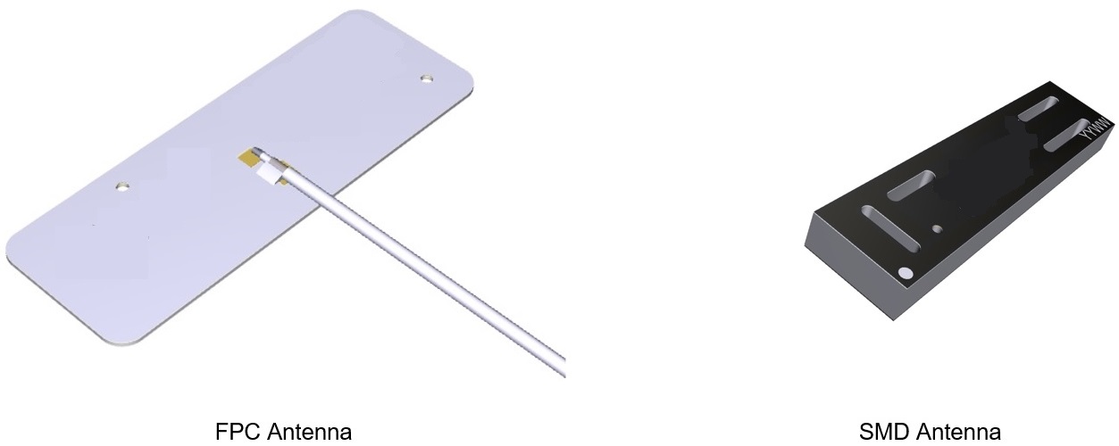
Surface mount device (SMD) antennas are useful in a design because they only take up a small amount of space, but there are alternatives. Antennas are available in flexible printed circuit (FPC) form, and these offer a useful design alternative for certain situations. Figure 5 shows both SMD and FPC antennas.
The FPC antenna connects to the circuit by its own RF coax cable with various connection options. You can use it in a different position within the device and will not take up any of the valuable space on the PCB. An FPC antenna can be bent or folded, which introduces many options for placing it. For example, it might be fixed to the inside of the device’s outer case.
Another important advantage to the FPC: it does not require a ground plane, which eases integration. The coax cable, however, of the FPC becomes part of the antenna. Thus, the routing of the cable should be designed with care. We recommend keeping this part of the antenna away from other components that might create noise and interference.
FPCs offer some useful benefits, but ultimately the decision between the FPC and the SMD antenna will depend upon the nature of the device, the manufacturing process for the device, and the quantity produced. The FPC antennas are fixed to a surface with adhesive, and each FPC antenna needs to be placed by hand. This makes FPCs suitable for smaller production runs with shorter timescales and hand assembly. SMD antennas can be placed on the PCB by a pick-and-place machine. These antennas are the better choice for devices that will be manufactured at larger volumes to reduce labor costs.
Conclusion
Generally, you will find designing easier if you use a low profile, high performance antenna. RF design is, however, complex and we recommend that you obtain advice from an RF specialist –- from inside or outside your company — before the finalizing a design. In most cases, the design will be tested in an anechoic chamber to check for performance and spurious emissions. This is the first step towards gaining certification in your design.
References
- Keyvan Yasami, “5G radios increase emphasis on compliance testing,” 5G Technology World, March 12, 2021. https://www.5gtechnologyworld.com/5g-radios-increase-emphasis-on-compliance-testing/
- Free Calculator for GCPW Transmission Lines, Antenova, https://blog.antenova.com/rf-transmission-line-calculator, registration required.
 Geoff Schulteis leads technical support for Antenova’s North American customer designs. He has over 20 years’ experience designing, integrating, and testing antenna systems for consumer products from R&D through manufacturing & commercial deployment. Geoff has designed antennas for various IoT applications ranging from 2G through 5G, earning him multiple patents.



Antenova publishes articles on antenna design. Here’s the latest.
https://blog.antenova.com/the-hidden-costs-of-trace-antennas
Here are the antenna types and how to calculate the wavelength and width of the antenna trace.
https://www.pcbonline.com/blog/pcb-antenna-basics.html