Learn the basics about SmartNICs, their design, and why they’ll be a crucial element in future networks.
In today’s connectivity-driven world, the data center has risen to a place of unprecedented importance. At the same time, technologies such as machine learning have placed intense computational demands and the requirement of faster data access for platforms such as 5G. These conditions place an unsustainable strain on data center infrastructure.
To address this issue, engineers are re-imagining the very hardware on which the data center is built. Out of this effort, one of the most important technologies that has emerged is the SmartNIC. Dell’Oro Group predicts that the SmartNIC market will become a $2B market by 2027.
In this article, we explore the SmartNIC; what it is, how it rose to prominence, and how it can be designed into a data center system to unlock future benefits.
What is a network interface card (NIC)?
Before understanding the SmartNIC, we must first discuss the fundamentals of its predecessor: the network interface card (NIC).
From a functional perspective, NICs have historically been an essential board or chip in computing systems, enabling connectivity in internet-connected systems. Also known as network adapters, NICs are used in computer systems, such as personal computers or servers, to establish a dedicated communications channel between the system and a data network. NICs act as translators, taking host memory buffers and formatting them for transmission over a network as structured packets, typically Ethernet. NICs also receive data packets from the network and turn them into memory buffers for applications on the host. Interestingly, all data transiting a network is always represented as character data, regardless of how complex the data structure is or the number of significant digits in a decimal number. This is because the earliest data networks, like ARPANET (1969), were built using standards that had been carried forward from earlier technologies like Telex (1933), which used a 5-bit code created in the 1870s by Emile Baudot. To be clear, ARPANET used 7-bit ASCII (1963); today, we use UTF-8 (8-bit), which is backward compatible with ASCII.
From a hardware perspective, a NIC consists of several key circuit blocks. Some of the most important blocks include a controller for processing received data and ports for a bus connection (e.g., PCIe) within the larger system. With this hardware, the NIC implements the physical layer circuitry necessary to communicate with a data-link-layer standard, such as Ethernet. Operating as an interface, NICs transmit signals at the physical layer and work to deliver the data packets at the network layer.
Now, servers rely on NICs to establish network connectivity, but current changes in the industry will render basic NICs obsolete for server use.
The rise of the SmartNIC
The proliferation of cloud computing and a general increase in internet traffic inundate data centers with growing data and computational tasks. Meanwhile, hardware is getting bogged down by the rise of data and compute-intensive applications such as machine learning, which are placing a greater strain on the computing hardware within the data center. To further confound the matter, the industry is simultaneously pushing towards faster data rates with technologies such as 5G, and soon 6G.
The result: existing data center hardware can no longer keep up with these demands. Workloads accelerate faster than CPUs can handle; the virtualization and microservices running in the data center are quickly becoming unmanageable.
Data center architects have realized that the processing requirements needed to serve the network have become too great for conventional NIC-based architectures. Instead, to achieve high performance without sacrificing power or complexity, we need to offload complex networking tasks from the server CPUs to dedicated accelerator blocks.
As many in the industry see it, the answer to these problems is the SmartNIC.
Inside a SmartNIC
At a high level, SmartNICs are NICs augmented with a programmable data processing unit (DPU) for network data acceleration and offloading. The name SmartNIC and DPU are often used interchangeably. The SmartNIC adds extra computing resources to the NIC to offload tasks from the host CPU, freeing up the host CPU for more important tasks.
Early SmartNIC implementations used register-driven ASIC logic. These designs tend to have higher performance in terms of extremely low latency, high packet throughput, and low power consumption — the latter ranging from 15 W to 35 W. Despite the performance benefits, however, they lacked the programmability and flexibility required, often utilizing esoteric command-line tools to set registers. They lacked any meaningful way to programmatically manage packet and flow complexity.
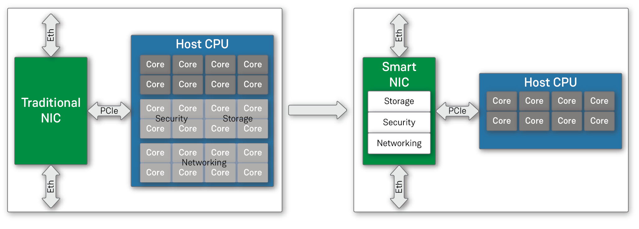
SmartNICs are used in many different deployments, including storage, security, and network processing. Some specific tasks that a SmartNIC may be responsible for include overlay tunneling protocols such as VxLAN and complex virtual switching from server processors. As shown in Figure 1, the eventual goal is to have a solution that consumes fewer host CPU processor cores and, at the same time, offers higher performance at a reduced cost.

Figure 1. Compared to a traditional NIC, a SmartNic adds storage, security, and networking features, removing them from the host CPU.
Taking a deeper look at a SmartNIC, we find that the programmable packet pipeline consists of many individual hardware accelerator blocks, all optimized for high-performance and low-power networking tasks. Depending on variables such as application and cost, there are many different SmartNIC implementations, each with its own benefits and tradeoffs.
One popular method for designing SmartNICs is to use a cluster of Arm cores. One of the major benefits of Arm core-based designs is the huge proliferation of existing tools, languages, and libraries. On top of this, these designs shine with respect to flexibility, featuring the best packet and flow complexity compared to other options.
FPGAs and SmartNICs
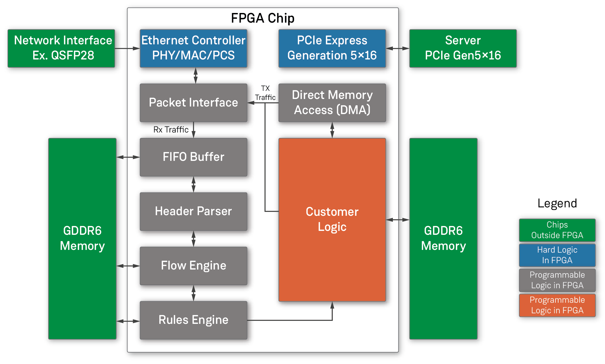
Many newer SmartNICs contain FPGAs, operating as an FPGA-based SmartNIC or an FPGA-Augmented SmartNIC. An FPGA-based SmartNIC, as shown in Figure 2, is a design that employs the expanded hardware programmability of FPGAs to build any data-plane functions required by the tasks offloaded to the SmartNIC. Because you can program an FPGA, you can tear down and reconfigure the FPGA’s data-plane functions at will and in real-time.
FPGAs can operate at hardware speeds as opposed to being limited by software, often offering several orders of magnitude in performance improvements. The large inherent parallelism in FPGAs leads to SmartNIC designs that exhibit high performance, high bandwidth, and high throughput.
The FPGA-based SmartNIC utilizes both hard logic for basic system input and output functions (blue boxes), as well as programmable soft-logic blocks (white box and orange) for advanced packet and network flow processing tasks. A huge region of programmable logic can handle custom functions loaded on demand or written and loaded in the field. These optional logic blocks might include wire-rate packet deduplication within a half-second window, load balancing of packets, and even flows or advanced security functions including unanchored string searches through the entire packet. Such searches might look for potentially thousands of strings in parallel.
FPGA-augmented SmartNICs, on the other hand, are systems that simply add an FPGA to an existing NIC complex. Based on the design, the NIC can be either an existing multicore SmartNIC or just a simple NIC ASIC. The FPGA can reside either behind or in front of the NIC chip complex or even out-of-band using a secondary PCIe bus.
Overall, SmartNICs that leverage FPGA technology can reap the benefits of good programmability and flexibility, as well as excellent latency and outstanding throughput. However, nothing is free; greater throughput and flexibility means the FPGA often draws more power than similar ASICs, which deliver substantially less performance.
SmartNIC Design Tips
Clearly, you have numerous choices and tradeoffs to balance when it comes to designing a SmartNIC. Ultimately, a successful SmartNIC design must:
- implement complex data-plane functions, including multiple match action processing, tunnel termination and origination, traffic metering, and traffic shaping.
- provide the host processor with per-flow statistics to inform network-tuning algorithms that optimize traffic flow.
- include a high-speed data plane that is programmable through either downloadable logic or code blocks to create a flexible architecture that can easily adapt to changing data plane requirements.
- work seamlessly with existing data center ecosystems.
To achieve these, it is highly unlikely that any one technology (i.e., ASIC, FPGA, or CPU) will lead to a “passable” SmartNIC. Instead, you should choose at least two technologies such as a combination of ASIC and FPGA. In practice, the best design will likely be one that marries all three design options along with a very high-performance network-on-chip to tie them together.
The SmartNIC, a network interface card with an integrated data processing unit (DPU), is gaining importance for use in data centers. Engineers can design SmartNICs with ASICs, Arm Cores, and/or FPGAs. Design choices come with several tradeoffs. All things considered, a successful SmartNIC design should be programmable, performant, and fit seamlessly within the rest of the system.
Scott Schweitzer, Director, Product Planning — SmartNICs, Achronix
Scott is a lifelong technology evangelist. He’s written software products for Apple’s App Store, built hardware, and managed programs for IBM, NEC, Myricom, Solarflare, Xilinx, and now Achronix. At Achronix, Scott’s role is the SmartNIC Product Planning Director. He focuses on accelerating networking and works with customers and partners to recognize new opportunities and define innovative products and solutions.


A key additional function of SmartNICs is the synchronization of time which will be forwarded to the underlying processors and databases. Precision time synchronization enables more efficient distributed database updates and optimization of parallel executed AI learning tasks. Precise time synchronization is achieved by IEEE1588 PTP time synchronization over Ethernet and by using precision timing clocks such as the SiT9514x Cascade Network Synchronizer, and ultra-stable timing references such as the SiT550x Elite X Super-TCXO from SiTime.