Bias control of PAs is crucial to ensure optimum radio performance under all conditions. Current sensing and temperature sensing provide the feedback needed to control the PA bias. The choice of sensing and biasing circuits brings design trade-offs.
5G base station power amplifiers (PAs) need biasing using a separate bias controller to maintain optimum performance over temperature. When designing a PA bias circuit, you can use current sensing with open-loop control or temperature feedback for closed-loop control. Each has advantages and disadvantages.
PAs play a crucial role in delivering RF power to a base station’s antenna. Average power for 5G can range from 2 W to 15 W, with peak power ranging from 16 W to 120 W. PAs must maintain linearity and efficiency over varying ambient temperatures as per the mission profile. Because PA bias current is a function of temperature, a PA needs bias-control circuitry to monitor and adjust the PA bias in response to temperature changes. Unlike handset PAs, an envelope-tracking-based adaptive biasing scheme may not be optimal owing to the higher RF power.
Figure 1 shows a typical block diagram of a PA and its bias controller in a transmit chain. The bias controller can be a separate package or integrated within the PA module. It operates by sensing the PA bias and adjusting it according to predefined control logic. We will explain the functionality and design challenges of the bias controller’s three main sub-components: the adjustable bias generation, the bias monitoring, and the control logic.
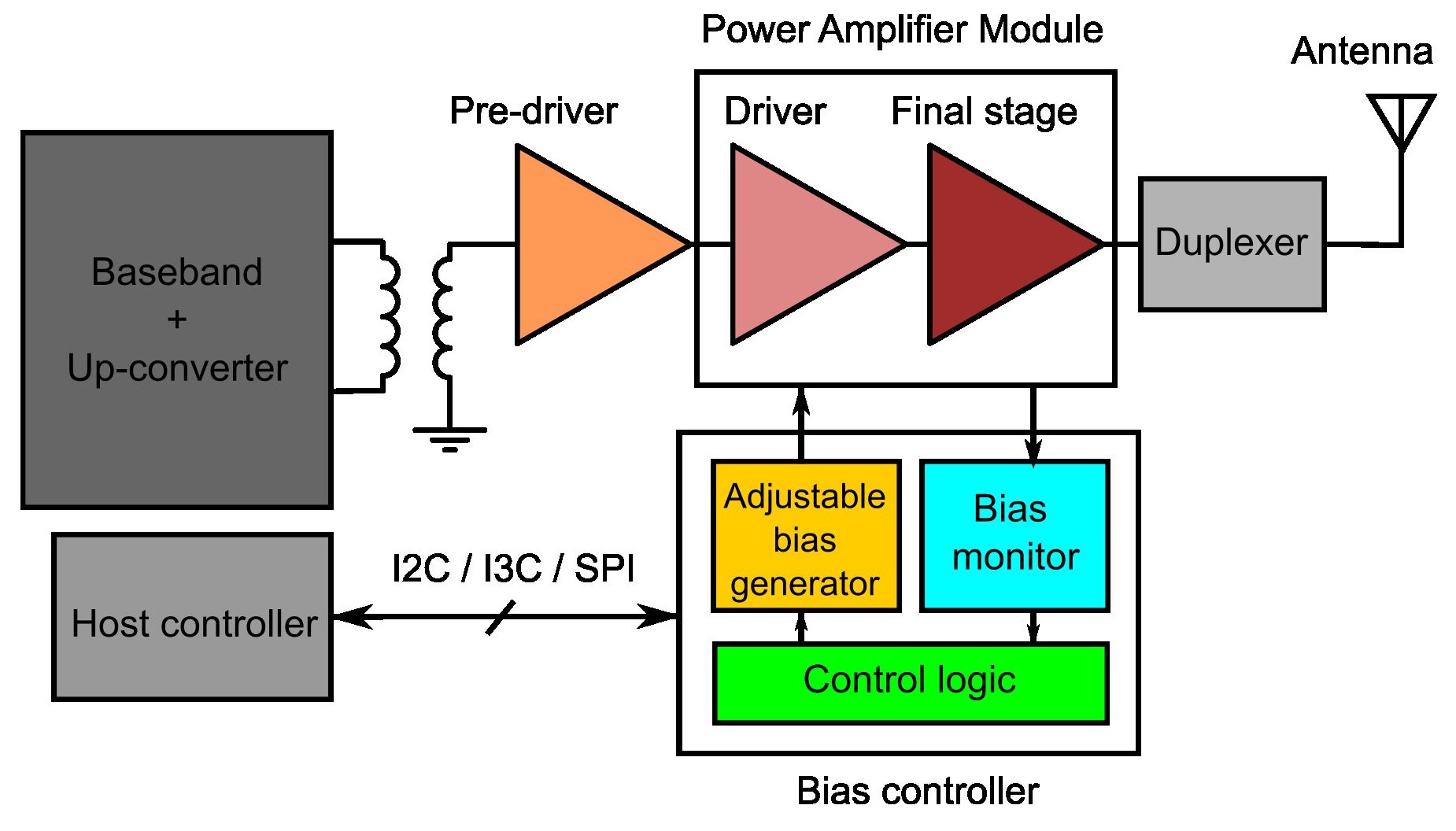
Figure 1. This block diagram of a transmitter chain shows a PA module and bias controller with major sub-components.
Adjustable bias generation
First, let’s describe PA biasing with an adjustable gate voltage. To deliver more than 40 dBm (10 W) output power, the circuit needs a high breakdown transistor. This helps to reduce the bias current with a reasonable device size, and it offers broadband input and output matches. Gallium-Nitride (GaN) devices are a popular choice because they typically operate at 28 V to 48 V drain voltage and provide good RF amplification and power-transfer efficiency. Other popular choices for lower power outputs are Gallium-Arsenide (GaAs) and laterally diffused metal-oxide-semiconductor (LDMOS).
These technologies are, however, expensive, offer lower levels of integration, and suffer from process variations as compared to their silicon counterparts. Under optimal biasing for amplification, the drain current of a transistor is, typically, a polynomial or an exponential function of its gate voltage. (We use the general terms “gate” and “drain” even for bipolar transistors where the equivalent terminals are “base” and “collector,” respectively.) This makes the bias current highly sensitive to gate voltage variations while it exhibits a weak dependence on the drain voltage. In many applications, the gate voltage is typically generated using current-mirror circuits that are themselves driven by precise supply-independent current sources. Furthermore, these current sources may have precise temperature slopes that can help achieve optimal performance over the operating temperature range. Typically, a high-precision digital-to-analog converter (DAC), controlled by the baseband processor, generates the gate voltage.
High die costs, large devices, poor level of integration, device mismatches, and part-to-part variations, however, make this approach impractical for typical base station PA devices based on GaN, GaAs, and LDMOS technologies. Instead, it is advantageous to have a separate bias controller chip implemented in a silicon-based technology that not only addresses many of these concerns, it offers robust digital integration.
The next important parameter is the DAC output voltage range, which depends on the transistor technology used in the PA. Table 1 outlines the gate bias voltage ranges for some of the popular technologies.

Table 1. Gate bias voltages for different PA transistor technologies. Although the exact voltages for different transistors may vary, this table provides a general idea of the voltage range applicable for that process.
A driver amplifier typically precedes the power amplifier. Many base-station implementations use different technologies for the PA and driver amplifier. For instance, the PA device may be a GaN transistor, while the driver amplifier may be a GaAs HBT or LDMOS device. Thus, the bias controller DAC needs both positive and negative voltage ranges. It also needs to handle a relatively large voltage while offering low-power transistors for compact digital implementation. Hence, a bipolar-CMOS-DMOS (BCDMOS) process that can handle large dual-rail output voltages and allows for digital system integration on the same die is a popular choice [1]. Modern BCDMOS processes are based on the relatively low-cost and readily available legacy 180 nm or 130 nm CMOS process nodes. The DAC resolution is also an important design parameter because it determines the bias precision. Here, most of the products on the market provide 12-bit DAC as standard, which leads to 1.2 mV and 2.4 mV bias resolution for 5 V and 10 V voltage-range, respectively.
Designers should also consider that the PA transistor remains in an off state before the circuit applies the drain bias. That’s especially important for depletion-mode HEMT devices that are fully on at zero gate bias and require an active turn-off (Table 1). Bias controllers also integrate a sequencing logic through a PA enable line that they assert through the power-good logic of the drain supply generator only after asserting the drain voltage. Also, for the depletion HEMTs, the drain voltage should be asserted after the negative supply to ensure that the transistor is off.
PA switching and the DAC
Now, let’s revisit the PA on-off switching through this DAC output. The transmitter switching time in a 5G radio should be a maximum of 10 µsec as specified by 3GPP [2]. The PA switching by itself needs to be much faster. The DAC output loaded with a large PA gate capacitance may, however, lead to a long settling time for the on-and-off voltages. Addressing this issue requires two DACs where the main DAC generates the on voltage while the reference DAC (REFDAC) generates the off voltage. These DACs then feed the gate terminal through an SPDT switch, shown in Figure 2. Large capacitors, typically 10 times the gate bias capacitor, further stabilize the voltage and act as charge reservoirs to assist in the rapid switching.
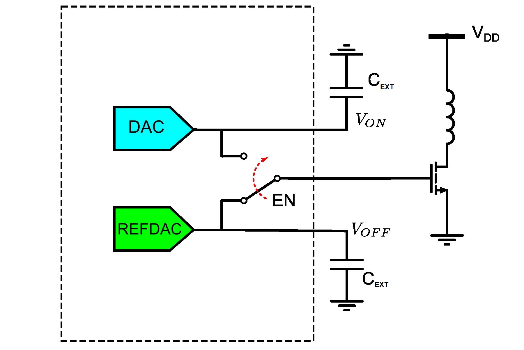
Figure 2. Rapid PA switching using an SPDT switch (EN signal) with two DACs generates ON and OFF voltages separately, each stored in external capacitors CEXT.
Modern high-efficiency base transceiver station (BTS) PAs use the Doherty architecture having two transistors per stage.
Commercial PA modules may integrate the driver and the final stage within a single package, thus doubling the number of transistors. One PA may require up to four DAC channels for its bias control. Multiple gates may share the reference DAC that generates the off voltage, while the on voltage may differ based on the transistor operation class. Now, modern massive-MIMO (mMIMO) radios may have 64 transmit channels, thus requiring 256 biasing channels. Integrating multiple channels within a package can reduce the bill-of-materials (BOM) and routing complexities. This is also an engineering challenge owing to the die size and thermal constraints.
Bias monitoring
Recall our original problem statement: the PA bias current is a function of temperature. We need to sense this variation to determine when and how much bias control the PA needs. This is accomplished by directly sensing the bias current and then adjusting the PA bias constant level, thus forming a closed-loop control. Another way is to sense the PA temperature and provide a bias voltage based on a predetermined look-up table. Hence, this method is an open-loop control. Each control method brings with it different challenges.
Figure 3 shows the current sensing for the closed-loop control. Here, we place a small external sense resistor between the supply and the choke inductor. Doing so results in a proportional voltage drop amplified with a current-sense amplifier and digitized with an analog-to-digital converter (ADC). This voltage is a direct measure of the current. Note that this voltage drop must be very small because it also reduces the PA voltage headroom, which directly impacts the output power and degrades the efficiency. For a 0.1 V drop with up to 1 A of bias current, a 100 mΩ sense resistor may be used. A 1 mA current sensing resolution implies a 100 μV voltage resolution for this readout, which is an extremely challenging precision to achieve given the supply voltage of 5 V to 48 V and the presence of direct and coupled noise.

Figure 3. Current sensing-based closed loop bias control of a PA transistor.
Therefore, such a sensor must have low noise performance, high gain, and a high common-mode rejection ratio (CMRR), along with proper decoupling and shielding. The sense nodes should also have a strong ESD rating and handle a voltage of 48 V.
Figure 3 shows the temperature sense in the open-loop control. Use an external temperature sensor, which could be a diode, positioned close to the PA. This sensor gets its power from the bias controller and the resulting output voltage goes to an ADC.
Based on the temperature reading, the control logic may bias the PA according to a predetermined look-up table (LUT). You can automate this process where the circuit periodically measures the temperature and updates the PA bias voltage. This may be a simpler arrangement than the current sensing method, though it comes with its own obstacles.
First, this method may not allow a precise control of the PA bias. The temperature variation at the sensor depends on its placement and proximity relative to the PA hotspots (Figure 4). The sensor may see a reduced temperature variation, which can impact the biasing precision. As the temperature is only an indirect measure of the bias current, careful calibration is needed to map the two parameters. On the other hand, temperature-based biasing can be used for all the devices, while the current sensor may be implemented on the supply of the main device only. In either of the schemes, the bias controller die should also have an internal temperature sensor to account for any local temperature variations.

Figure 4. The external bipolar transistor functions as a temperature sensor, used for open-loop bias control of a PA.
Control logic
The control logic adjusts the bias voltage based on the sensed current or temperature. This control logic can’t be hard-coded; it must be programmable to account for the PA’s process variations. This is one reason why an analog auto-control can’t be used for the closed-loop. The control logic may be implemented in an integrated microprocessor, though this is often overkill. An optimum solution is to program the logic in the BTS host controller, which then configures the bias controller through a digital interface such as I2C or SPI (see Figure 1). This may enable radio manufacturers and operators to optimize the control logic based on their mission constraints.
Specifically for open-loop control, a look-up table (LUT) is sometimes integrated within the bias controller’s non-volatile memory to map the temperature to the required PA bias, which reduces the load on the host controller. In such implementations, the LUT may also integrate interpolation logic and an autonomous control mode based on the LUT map.
Summary
While the essential bias-control principle remains the same, there are myriad ways that differ in their implementation details and thus require careful consideration from the system perspective. For the system integration, it is important to understand the bias controller features and their associated trade-offs across the three discussed sub-components to select the best applicable solution. It is equally important for the IC designers to understand the different challenges and the overall system before designing these solutions.
References
- A. Andreini, C. Contiero, and P. Galbiati, “A new integrated silicon gate technology combining bipolar linear, CMOS logic, and DMOS power parts,” IEEE Transactions on Electron Devices, vol. 33, no. 12, pp. 2025-2030, 1986.
- ETSI, “3GPP TS 38.104 Version 17.12.0, 5G; NR; Base Station (BS) radio transmission and reception,” 2024.


Tell Us What You Think!