The Certus-NX FPGA from Lattice Semiconductor includes fast I/O and a hardened PCIe interface for connecting to local devices and to the outside world.
IoT devices, robots, consumer devices, asset trackers, and other devices need more on-board computing power than ever before. With the need for fast decision making, devices often can’t wait for a remote computer to analyze data and make decisions. Besides, why burden a remote computer with local decisions? That’s there the Certus-NX FPGA from Lattice Semiconductor comes in.
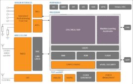
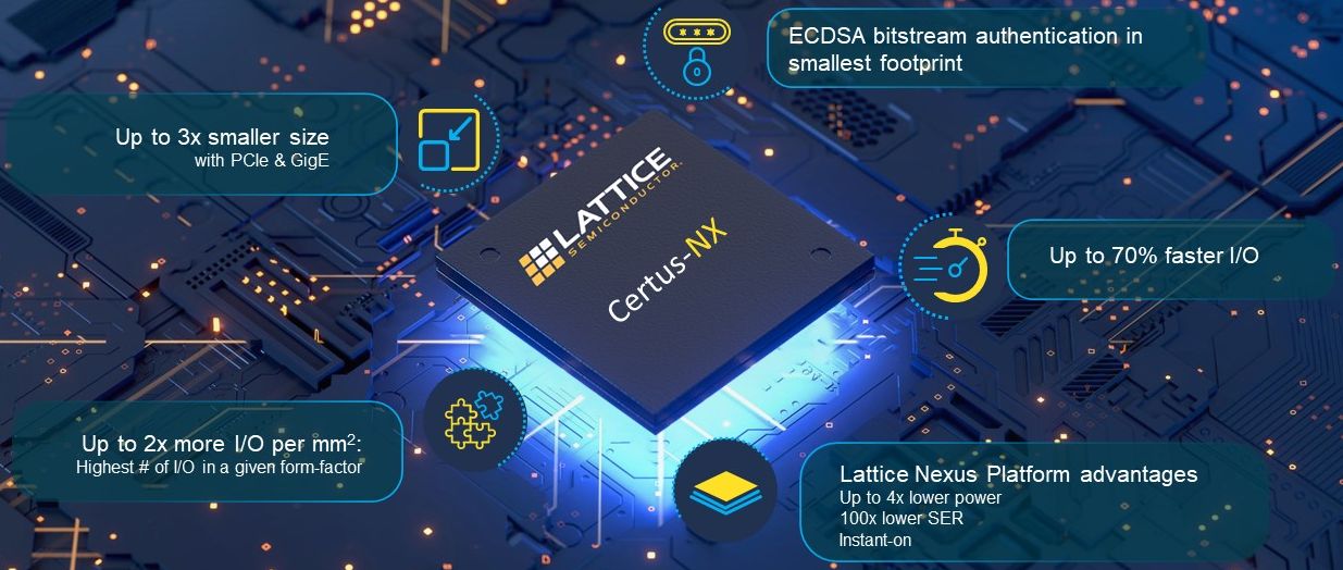 The 36mm2 size of the Certus-NX package lets you cram more processing power into existing space or it lets you reduce the size of designs that don’t have predefined space requirements. Offered in two version, the Certus-NX has either 17 k or 39 k logic cells for you to embed functionality. A hardened single PCIe Gen 2 (5 Mb/s) I/O bus lane lets you connect the FPGA to other devices such as cellular or Wi-Fi modules for wireless network connectivity. The FPGA’s 192 channels of 1.5 Gb/s programmable I/O lets you control motors, read sensors, and connect to other communications buses such as gigabit Ethernet. Lattice provides the IP needed for communications buses that you embed into the I/O. It also contains two lanes of 1.25 Gbps Serial Gigabit Media Independent Interface (SGMII) for 10/100/1000 Mb or Gigabit Ethernet, two ADCs (each 12-bit, 1 MSa/s) and a phase-locked loop.
 Many devices need to remain in a sleep mode as long as possible to maximize battery life. The Certus-NX addresses that issue with an “instant on” feature that brings up the I/O in less time that the core logic. Lattice claims that the configuration times listed in the table beat competitors by a factor of four.
From a security standpoint, the Certus-NX includes Elliptic Curve Digital Signature Algorithm (ECDSA) for authentication. ECDSA uses public and private authentication keys where the user holds the private key. This even if a device containing a Certus-NX FPGA falls into the wrong hands, the authentication key is stored remotely.
| Feature | LFD2NX-17 | LFD2NX-40 |
| Logic Cells | 17 k | 39 k |
| Embedded Memory (EBR) Bits (kb) | 432 | 1512 |
| Large Memory (LRAM) Bits (kb) | 2560 | 1024 |
| 18 × 18 Multipliers | 24 | 56 |
| ADC Blocks | 2 | 2 |
| GPLL | 2 | 3 |
| 5 Gb/s PCIe Gen2 Hard IP | — | 1 |
| Full-chip Configuration Time (ms) | 8 | 14 |
| I/O Configuration Time (ms) | 3 | 3 |
Low-power FPGAs could find new use cases once 3GPP is ratified in 2021. Release 17 address IoT support in 5G New Radio.


Tell Us What You Think!