They’re all related. Changing one can affect the others, explains Bert Simonovich in an interview with EE World.
As digital data streams increase in speed, frequencies rise, and time-per-bit shrinks. That leads to signal integrity issues, which get more and more complex each time the data rates increase. Those signals travel over a circuit board. How do circuit board materials and construction affect the integrity of signals that travel across the board?
To learn more, we spoke with Lambert (Bert) Simonovich of Lamsim Enterprises. Bert designs high-speed PCBs and backplanes. He has done a lot of research into how PCB construction, particularly trace roughness, glass weave, and stackup impacts the quality of digital signals. Bert has written numerous papers on these topics and presented them at conferences such as DesignCon. At the time of this recording, Bert is a nominee for the 2024 DesignCon Engineer of the Year. An edited version of the transcript appears below the video.
EE World: Bert, thank you for speaking with EE World, can you give the viewers an introduction into the physics of PCBs and how their construction affects signal integrity when simulating a design?
 Simonovich: I’m involved with signal integrity, high-speed signal integrity, mainly. Along the way, I have come across how material properties impact designs. I’ve done a lot of my own research on conductor roughness a few years ago earlier, and that was the main focus. Since then, I’ve realized that the conductor roughness affects not only the loss of the actual metal or the conductors, it also has an impact on the dielectric properties of the material and these dielectric properties are used to model your design. If you don’t account for them, then typically you may end up with the wrong result, not as accurate answer in your simulations. So, I kind of put roughness affecting your PCB laminate more at the top of the list because it has an impact on all of that.
The actual dielectric material has anisotropic. It’s anisotropic properties, meaning the electric fields react differently in the dielectric, depending on the axis that it’s being excited with. The impact there is how the permittivity or dielectric constant is derived or published that board shops use to define your stackup and do the impedance calculations. Depending on the test method used, the dielectric constant (Dk) will be either in plane what they call or out of plane. If they’re in plane, and you try to use it for transmission-line modeling, you’ll get the wrong impedance. When you build the board, it may fail the tolerance mass. So this is the topic I’ll be discussing at DesignCon this year. I’ve done some research on and I’ve come up with a way to convert between one and the other based on the datasheet, and that’s what the presentation will be about.
So that’s that material properties, then a high speed we start thinking about fiber weave effect. When we have differential pairs, connecting serial links, and you can experience fiber weave effect, starts to impact things sort of 10 gig and above. Because the higher you go [in speed], the less margin you have in your design, and what the fiber weave effect does, it creates a skew between the one trace and the other like timing skew. That affects your budget. You’d end up with extra loss potentially in your design.
People can mitigate that with different techniques. They have what they call spread-weave glass that spreads the actual fibers of fiberglass cloth in the resin. That helps to mitigate it to equalize the decay. They [the PCB shop] also can rotate the artwork when they do the design and, and different things. So and then there’s issues if you rotate depending on the angle of rotation, then you can create other effects called the Floquet-Bloch effect, where you can get tiny little resonances in the insertion loss. So, it all ties together, how you start looking at it. That’s just a general overview of how everything is related, just traced surface roughness adds impedance to a transmission line, thereby affecting current flow and magnetic fields.
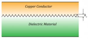
As you mentioned, the copper bank gets put down, it’s not perfectly smooth. In fact, they intentionally make it rougher. So they get good adhesion to the dielectric material. So, in some sense, it’s what’s good for mechanical bonding and peel strength to keep the traces on the board for rework, or everything goes against signal integrity, as we go up in speed. So, effectively, adding roughness increases the loss of your signal, between the two interconnects or your net, basically. And along the way, the roughness itself, it also adds some additional delay to the circuit, there’s more of an inductive effect as well. It could affect some timing. Also, if you’re doing RF design, the roughness, not as concerned with the loss there, but it does affect the dielectric in that perspective. So, there are two ways of looking at it, the circuit model, so to speak, where electrons are flowing through conductors, that’s what people use in a model. To a certain point, that’s a good enough model. But electrically and magnetically, it’s the wave propagation that’s guided by the transmission line of the copper and the reference planes. Adding roughness starts to impede that propagation. So, it adds some delay, but it also absorbs some of the energy. And, some sort of scattering so electromagnetically, you’re attenuating that signal going through the old, the old roughness kind of model was, you know, has like peaks and valleys and current would go above and below and it would increase the loss because you make the path longer.
That’s how people used to think of the roughness. You’ve got a longer path that accounts for the extra loss. But that’s not actually how physics works. If that was the case, you’d be violating the physics laws of speed of light have to go faster to to get there. So essentially, roughness is no good for loss. And what we try to do for the higher speeds is to get less rough foil and have different bonding techniques to get good bonding, yet have a fairly smooth surface in the copper itself now, so that’s what we’re trying to do.
We’re getting into the higher speeds, certainly at above 20 gig, 25 gig, 56 gig, 112 gig. As the system’s going every couple of years it seems to be pushing higher and higher. Every time data rates increase, a new physics problem arises. One of those is fiber weave effects.
EE World: PCBs consist of fiber strands that give them strength. But how do those fiber strands impact signal integrity?
 Simonovich: Particularly in differential signals, when we fabricate the actual printed circuit board laminate itself, the material, it’s made of a mixture of fiberglass woven cloth. So just like your cotton cloth is woven, and it’s like a grid you can see. It weaves up and down x and y, so they call that the warp and the weft or the fill direction. The weave pattern, it’s like a checkerboard, for lack of anything better. You have glass fibers running x and y but you’ll end up with some space between — resin, like open space, if you actually looked at it.
When they make the actual laminate, they mix, they impregnate that cloth with resin and they call that prepreg, pre impregnated. It’s what they call it, and it’s partially cured. They take these prepreg sheets, they’re certain thicknesses, and they can vary, you can put different sheets together to build up your thicknesses for your laminate, they put copper on each side of the sheets, they press it under heat and pressure, and it’s cured. That’s what they call core laminates. It’s already cured with copper on it. Then they’ll etch the pattern of your circuit on each side or one side depending on what it is.
When you get a differential pair, there are two traces that are close together usually, and then routed together along the surface of the of the core.
Now remember, I said has a grid pattern of the fibers going x and y. If one trace lands on the fibers going X or Y sets just going in the x direction, if one trace is landing perfectly on that fiber over the entire length, but the other trace now is over mostly of the resin, where the open windows are between those two, the x fiber traces will have a pitch. If your transmission lines are not on the same pitch, one trace will be mostly on glass, the other will be mostly over resin.
The dielectric constant affects the speed of the signal as it propagates down. If you have two different dielectric constants, because the dielectric constant of glass is higher than the dielectric constant of a resin, the positive end of the trace will travel at a slower speed if it’s over a glass than over the resin. And that difference in speed is what we call the skew if you like the timing skew.
If you have a differential pair, you’ve got a plus signal and a minus signal traveling down the pair. If you get one traveling faster than the other, then when it gets to the receiver, they’re not perfectly matched. That becomes differential. When there’s skew, that’s when you get what we call mode conversion from a differential signal to a common signal. It’s the amount of skew. Now, having a common signal on a differential pair is not good because it would radiate. It’s common to both and that’s why they put chokes on and do things.
So, you try to not have any kind of skew in your differential pair.
A main contributor to skew is fiber weave effect in the board. So that’s why it’s an issue. Because the two traces are seeing two different dielectric constants, and the speeds are different. So what we do is we mitigate that. There are different ways to do it. The easiest is you just, not have perfectly straight traces if you can.
If you can meander the traces and don’t have them running perfectly straight. Or if you can’t, if they have to be straight, then you rotate the either the artwork on the board, or you rotate the actual panel, when they fabricate the board at the board shop, they can rotate the angle, you know of the board so that the traces, if they’re straight, they will not run exactly parallel now to the actual fiber weave, they’ll run on an angle, so you won’t get that effect. So that’s what people have been doing. Now they have what they call spread-weave glass, where they actually spread the fibers. After they weave it, they’ll spread, at the fill in, the areas that were sort of open. In the weave got a checkerboard. They call that spread we’d glass. So that’ll help.
EE World: So by spread weave Do you mean that the weaves, the glass strands one strand to the next to the next to the next, the distance between them will vary somewhat deliberately?
Simonovich: When you weave any cloth when you do the weave, they call the warp and the weft. Warp is the say it’s the vertical or the y direction, and the weft or the field is the x direction. Then you have different strands like what they had, the strand here, and then a certain distance needed to have another strand. So it’s between the pitches of the strands, you have the open space. So normally, the warp is the ones that that’s the length of the cloth that gets drawn. And the weft is the stuff that goes across each time.
Then the weft or the fill, they’ll spread the fill yarns to fill in that space. The Warp ones don’t tend to spread. Mostly, they [the PCB shop] just spread it out just to fill in that gap between it so they could spread both ways or just the one. Regardless, it’s a spread weave. We tried to make it more homogeneous between the two dielectrics.
EE World: How does rotating the entire circuit image relative to the grid improve signal integrity in differential pairs?
Simonovich: That introduces another issue, because now if you’re rotating your panel, depending on the angle of rotation, it could cause another bit of an issue from signal integrity because these fiber weaves, when they get woven, they go above and below each other. So they have where they cross is like a knuckle, what we call like a knuckle. That’s where the x and y overlap sort of thing.
If you have a straight trace, on an angle, eventually that trace is going to cross the knuckles periodically. Where the knuckles are, that little point knuckle that has even additional sort of extra decay, so adds extra capacitance, essentially, in it. They call that periodic loading. So depending on the angle, you’ll get the loading at a different period sort of thing. What it really looks like an insertion loss, you get a tiny little resonant blip, a very high Q blip, it’s not very deep, but it’s a blip. If that blip happens to occur at your Nyquist frequency of your bit rate, you can add more loss of that Nyquist frequency that were we look for.
So you have to be cognizant now of the angle and it’s a simple calculation. You can get the warp and the weft pitch from the standards, you know what those pitches are. You just use trigonometry to figure that distance out and you can work back and you can predict where that resonance will occur. It works well and people have done papers on it. I’ve experienced that myself recently in some characterization work. I’ve seen the blips and when I work back the math that happens exactly right where it’s supposed to. So it’s there. So just trying to make sure that blip does well away from any important frequency that you want. That would determine any angle of rotation that you would do to mitigate your fiber weave. That’s how they’re tied together — you kind of fix one thing, but you could create another problem if you’re not aware of this other part.
EE World: Bert, earlier, you mentioned stackup. Most complex circuit boards have more than two layers. Eight, ten, and twelve are quite common. How does the stacking of those layers affect signals on the board?
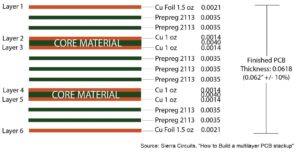
 Simonovich: To build a stack up, it’s really what it says, I mentioned before we how we made the cores with a double-sided copper on it. If you’re building a multi-layer board, it’s a stack up. You have a series of cores that you’re putting together. But to glue those double-sided cores together, you still use the prepreg. So now a stack up is, if you sort of start at the top, you have a top layer, you’ll have a prepreg or core, let’s just call it prepreg. Then you’ll have another double-sided core, then a prepreg, a double sided core, and it goes down, down, down to the number of layers that you have.
That in itself is not a big deal. When you build a stack up, it’s important to have symmetry above the center. So, whatever is above the center of the stack up has to be the same below as far as the copper thickness, the dielectric thickness needs all to be symmetrical. So typically, when we make a stackup, it’s an even number of layers. You won’t see an odd number of layers. It will be even numbers. That’s because the need to maintain the symmetry.
What we try to do, is to keep the on cores, the same thickness of copper on each side. We call that copper weight.
The PCB world is really strange. They often call weight of copper for thickness, that half-ounce copper, one-ounce copper has a certain thickness that represents the number of ounces. That is, what the thickness would be of ounces per square foot. A half ounce of copper is roughly about 0.7 mils. One ounce is 1.4 mils. So, you’ll see stackups talk about ounces rather than thicknesses. When you see ounce, you know it’s roughly that thickness. That’s where some confusion happens: How do you get thickness from ounces? But that’s where it comes from.
So that defines how you actually build the stack up. But you can’t go, forever with your thickness, obviously.
With every board now you have through-hole drills, they drill through the board, so they can mount components or connect layer to layer with the vias. These drills have a certain size, but then we run into the aspect ratio, what board shops call in order to ensure good plating for all the way through the via barrel from top to bottom. They have an aspect ratio.
An aspect ratio is the ratio of the drill size to the thickness of the board. A 10 mil drill, you have 10 to one. It’s like 100 mil type of thickness, right? So it’s a ratio of the board thickness to drill size, essentially. Board shops will have a limit of what they claim they can work towards. Most board shops do ten-to-one. That’s sort of pretty good. Higher-end board shops can go higher, say 15 and Some may be 20-to-1 depending on their process. That’ll define the maximum thickness of your board — the aspect ratio — because you can only have a certain size your drill size works in. That’ll impact your pitch of your parts that you put on, depending on what the pin patterns are, what can go on there? So it all sort of ties together. There’s a dance between boards board thickness, how many layers, component pitches, and how you do things. It all works together that way.
EE World: Bert Simonovich of Lamsim Enterprises, thank you for explaining how PCB copper roughness, fiber-weave effects, and stackup affect the signal integrity of high-speed digital data streams. For EE World. I’m senior technical editor Martin Rowe. Thank you for watching.


Good report