If you think antennas must live “outside” a circuit, think again: they can also be housed in a small package adjacent to the active components they serve.
The previous part established the context and rationale for AiP; this part continues the exploration.
Who are some of the AiP technology suppliers or OEMs?
ASE, a leading provider of semiconductor packaging and test services, provides both sophisticated design tools and production expertise.
Another leading vendor, Amkor Technology, has cutting-edge AiP and AoP technology that has already been deployed and offers fully integrated 5G NR (new radio) millimeter wave and sub-6 GHz RF modules for smartphones and other mobile devices. These mmWave antenna modules deliver capabilities across several spectrum bands in a very compact footprint that is well-suited for integration in mobile devices.
French-based InsightSIP is a product OEM offering standard System-in-Package products, some of which include the antenna (more on this later).
These are just a few of the sources, of course.
Is there only one type of AiP arrangement?
There are three key types:
- Flip Chip Ball Grid Array (FCBGA) based AiP: here, the FCBGA-based AiP includes an RF chip mounted on the bottom of a ball grid array (BGA) substrate and an antenna array formed on top of the substrate (Figure 1).

Figure 1. The FCBGA-based AiP has the RF chip mounted on the bottom of a ball grid array (BGA) substrate and an antenna array formed on top of the substrate (image: ASE).
- AiP Modules: In this approach used with some smartphones, the RF chip is mounted on top of a multi-layer (typically with 12 or more layers) antenna board. With an antenna array formed on the bottom side. It is designed to include a connector that simultaneously carries multiple high-frequency signals to the phone’s main board via a flexible printed circuit board (Figure 2).
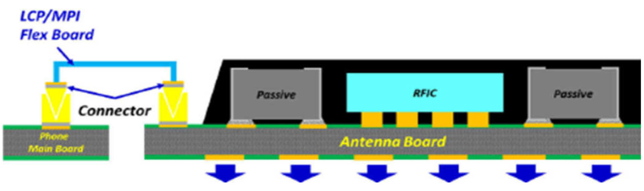
Figure 2. In some AiP modules used in smartphones, the RF chip is mounted on top of a multi-layer (typically with 12 or more layers) antenna board (image: ASE).
- Hybrid substrate-based AiP: This packaging architecture mounts the RF chip on top of a hybrid substrate including a typical BT substrate and an antenna flexible printed circuit (FPC). The antenna FPC is built from low dielectric constant (Dk)/dissipation factor (Df) materials that enable the lowest possible signal loss for high-frequency applications (Figure 3) [note: bismaleimide triazine (BT) contains a mixture of bismaleimide and cyanate ester and is one of the most commonly used resins in the manufacturing of printed circuit boards].
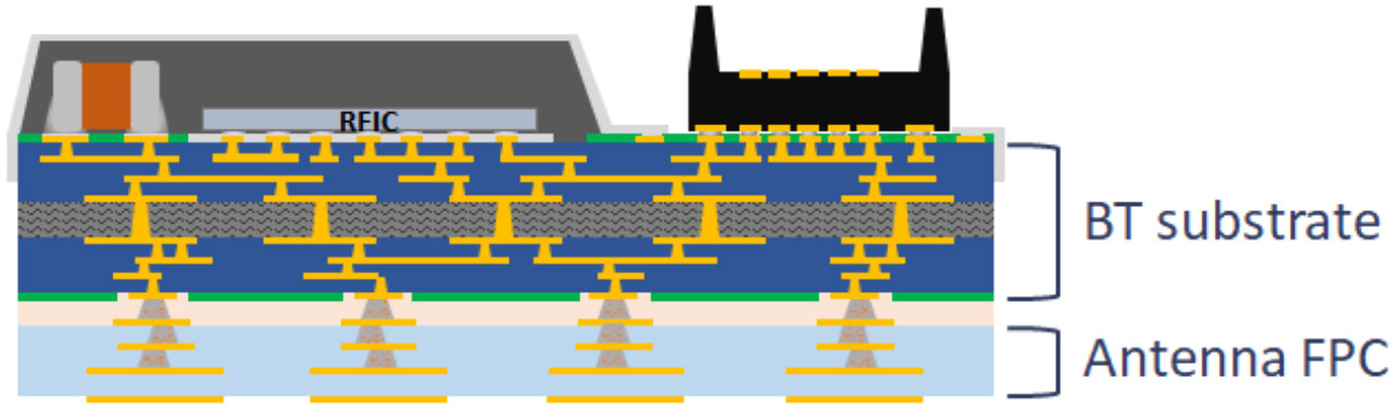
Figure 3. Hybrid substrate-based AiP mounts the RF chip on top of a hybrid substrate including a typical BT substrate and an antenna flexible printed circuit (image: ASE).
What are some of the other major technical factors leading to the development and implementation of AiP? What is making them viable at this time?
First, there have been many packaging innovations in the past decades, not only for monolithic ICs themselves, for also for co-packaged die, modules, and similar. These are occurring in areas such as power-regulator ICs with on-board FETS, RF interfaces with co-processors, stacked die, memory devices, and more. The IC industry has not only enhanced IC packages, but also enabled specialty packages that house one or more die plus associated discrete active and passive components.
Is there more?
Absolutely. Advanced modeling and simulation tools have been developed and can run sophisticated applications in a reasonable time. This is critical because the entire AiP device performance – electrical, RF, mechanical, thermal, and manufacturability – must be thoroughly evaluated before fabrication begins, as respins are costly and time-consuming. These tools instill a high level of confidence in assuring that the device will not only work, but will meet specifications across multiple perspectives.
As mentioned earlier, of course, there are consequences of the laws of physics and the electromagnetic spectrum, as frequencies increase and wavelengths shrink.
What package sizes and types are used for AiP?
It varies with the specific manufacturing vendor. For example, Amkor Technology notes that they can produce body sizes up to 29.0 mm × 4.0 mm, with up to 14 substrate layers.
RF design often needs shielding to prevent crosstalk, interference, and noise between the circuit and external elements; how does AiP handle that?
Vendors such as Amkor offer “compartmental” shielding using vertical wire and wire fence technologies, along with partial (selective) conformal shielding. It gets more complicated: RF shielding techniques include dual-side mold, conformal shield, compartment shield using laser trench and paste filling technology, partial molding, selective conformal shielding, and hybrid SiP designs. These techniques implement a variety of materials including conductive lids, cored, coreless and low coefficient of thermal expansion (CTE) substrates, and innovative conformal-shielding materials.
Can you give an example of an actual standard AiP device for sale?
The ISP4520 from InsightSIP (France) is highly miniaturized LGA (land grid array) module measuring just 9.8 × 17.2 × 1.95 mm, for the upper ISM Bands in the region 800 to 900 MHz, Figure 4. There are three variations of the ISP4520, each one tailored for different international RF standards and markets.
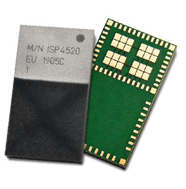
Figure 4. The ISP4520 supports the 800 to 900 MHz upper ISM band and includes the necessary antenna in its 9.8 × 17.2 × 1.95 mm LGA package (image: InsightSIP).
What’s in the ISP4520?
It uses the Semtech SX126x LoRa transceiver series and Nordic Semiconductor nRF52832 BLE chip (Figure 5). The module integrates a Cortex™ M4 CPU, flash and RAM memory, decoupling capacitors, 32-MHz crystals for LoRa and BLE and 32.768 kHz crystal for BLE, and DC-DC converters in addition to the wireless SoCs.
On the RF side, the ISP4520 also integrates the matching circuits for LoRa and BLE transmitters and receivers, a switch for Rx/Tx LoRa transmissions, and a diplexer with a common antenna for LoRa and BLE operation. The user interface is an SPI connection.
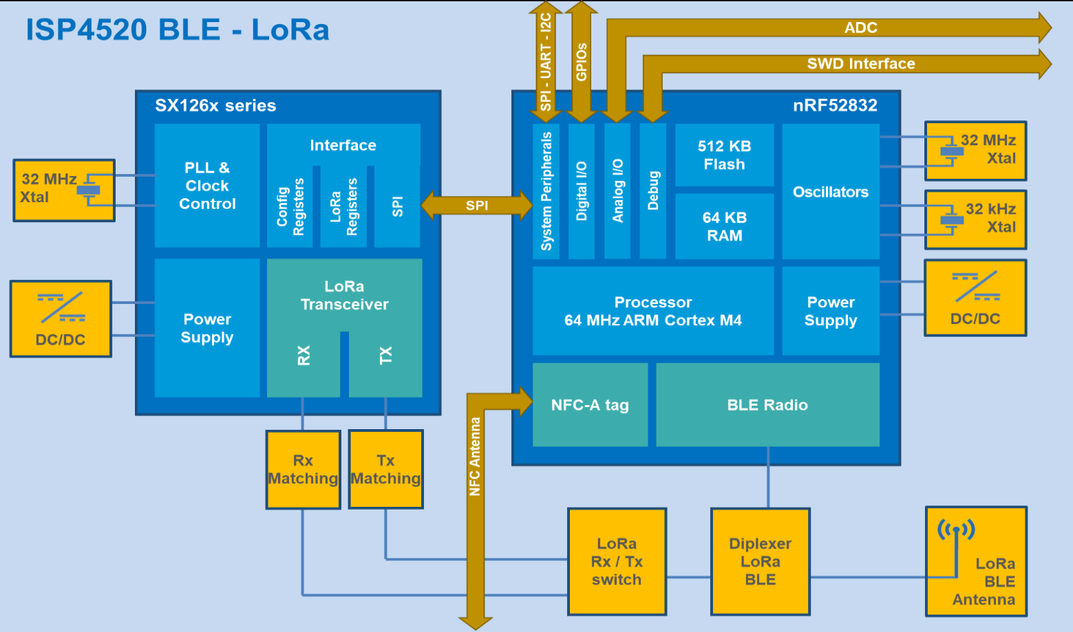
Figure 5. The internal complexity and integration of the ISP4520 shows its “completeness” for the target application (image: InsightSIP).
Of course, the performance and radiation pattern of the antenna is critical. Among the illustrative graphs, InsightSIP offers one for the ISP4520 LoRa radiation pattern with the unit mounted in the top corner of an application circuit board (Figure 6).
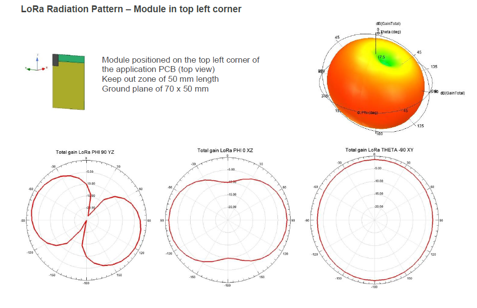
Figure 6. The effectiveness of the design and its execution is confirmed by the LoRa antenna radiation pattern (image: InsightSIP).
What are some of the AiP device test challenges?
Many 5G designs for mmWave deployment use AiP technology to improve radio frequency (RF) performance. Engineers developing AiP at mmWave frequencies must address several key challenges, such as greater path loss, wider bandwidths, and more complex signal generation and analysis.
For example, Keysight’s solution for testing millimeter-wave AiP technology comprises signal generation and signal analysis hardware coupled with measurement application and signal generation software. This integrated testing environment is specifically designed to help you solve your most complex mmWave AiP over-the-air measurement challenges.
Q: Can you be more specific?
TMYTEK, a user of AiP devices for their mmWave NR beamforming-development tools, needed a test solution with high output power, ultra-low phase noise, wide analysis bandwidth, and high dynamic range to perform over-the-air (OTA) testing at mmWave frequencies for 5G and satellite applications. They used a Keysight VXG microwave signal generator with Keysight PathWave signal generation software to generate high output power and compensate for system loss. The Keysight UXA-Series signal analyzer received the 5G New Radio (NR) signal through the AiP to analyze the signal (Figure 7).
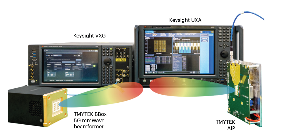
Figure 7. This over-the-air lab test setup was used in conjunction with advanced instrumentation and software to test the performance of the TMYTEK BBox 5G mmWave beamformer with an embedded AiP device (image: Keysight Technologies).
The TMYTEK BBox 5G mmWave beamformer transmits the 5G NR signal from the VXG microwave signal generator in the mmWave band with beamforming. TMYTEK’s AiP module provides the signal to the UXA-Series signal analyzer.
Using this arrangement, TMYTEK can characterize the AiP because of its high dynamic range and accurate error vector magnitude (EVM) performance. The Keysight PathWave signal generation and Keysight PathWave X-Series measurement application software support various emerging communication formats to accelerate the design and test workflow.
Conclusion
Antenna-in-Package technology is a viable approach in some situations to the challenges of higher RF integration, especially but not limited to frequencies above 10 GHz. It requires significant up-front design effort, planning, and implementation effort, as well as a good fit with respect to frequencies, thermal considerations, device RF power, device DC power, and many other factors to create a successful and viable design.
In many circumstances, it offers a solution that is much more attractive than using a set of ICs or modules with a discrete antenna. However, there are also applications where a conventional, discrete out-of-package antenna is a better solution with respect to optimization, vendors, costs, and risks.
Related EE World Content
Demonstrating antenna diversity, Part 1: The challenges
Demonstrating antenna diversity, Part 2: The PIFA
Demonstrating antenna diversity, Part 3: The Yagi antenna
Test methods for mmWave AiP designs bring tradeoffs
Wearable antennas target UWB frequencies
Lens antennas focus multiple wireless beams
What materials can be used to make miniature antennas?
The basics of dielectric resonator antennas
Software tool helps designers place antennas in design
5 tips for designing with embedded antennas
References and Resources
ASE, “Antenna in Package (AiP)”
Amkor Technology, “Antenna in Package (AiP) – Antenna on Package (AoP)”
Amkor Technology, “System in Package”
Chip Scale Review, “Antenna in AiP technology for 5G growth”
AnySilicon, “Understanding Antenna in Package Design”
InsightSIP, “Case Study: Quad Band GSM integrated antenna”
InsightSIP,“Case Study: ISP090401 2.4 GHz Transceiver Module with Integrated Antenna (Preliminary)”
InsightSIP, “ISP4250 Data Sheet”
InsightSIP, “ISP4520 Application note AN200601: LoRa Range versus PCB size and
module position”
Keysight Technologies,”Millimeter Wave Antenna-in-Package Test”
Keysight Technologies,”Accelerate AiP Design Integration”
TMYTEK, “BBox™ 5G mmWave NR Beamforming Development Tool”
Wiley/King Abdullah University of Science and Technology, “Antenna-in-package Designs in Multilayered Low-temperature Co-fired Ceramic Platforms”
IEEE, “Antenna-in-Package Technology and Applications

Tell Us What You Think!